


 FOR FURTHER INFORMATIONS: Stefano Rampino - +39 0521269282 - stefano.rampino@imem.cnr.it
Low-Temperature Pulsed electron deposition (LT-PED) is a physical vapour deposition technique (PVD) capable to grow good-crystalline films at low temperature and from a single target. The most important feature of LT-PED is to transfer the stoichiometry of the target into the deposited film, independently on the material phase diagram. By means of pulsed electron beams with a huge power-density (some 108 W/cm2), the technique delivers an astonishing amount of energy to the target material in a very short time (in the order of 100 ns). The LT-PED power density is orders of magnitude higher than the one necessary to evaporate materials (105 -106 W/cm2), so bringing to non-equilibrium heating of the target surface. Therefore, the target material is suddenly transformed into plasma without undergoing any phase transition: congruent evaporation is achieved even for incongruent melting point material. This phenomenon is called “ablation”. In this way, the composition of the target is transferred to the plasma and then to the film. Since temperature of the plasma is incredibly high (thousands of K), plasma species are extremely energetic (up to 10 eV). When these particles approach the substrate, the film grows with a good crystallinity even for low substrate temperature, since the inner energy of the species is sufficiently high for increasing the adatom mobility. For this reason, LT-PED is most suitable for those multi-component semiconductors, complex metal-oxides and alloys which usually form different phases, or solid state solutions of these phases, as a function of the composition and the growth temperature. Incongruent-melting-point material cannot be grown by means of co-evaporation or sputtering methods without applying the right temperature to form the wanted phase and neither from a single target with a good control in the composition. Indeed, by means of LT-PED it is possible to grow the correct phase by a stoichiometric single target and at a lower temperature. A small thermal evaporation process occurring at the target surface is unavoidable, but it can be minimized by maximizing the power density of the e-beam. Several materials had been reported to be deposited by means of pulsed electron deposition: ZnO-based semiconductors, composites CoFe2O4-BiFeO3, hydroxyapatite and other oxides, FeS2 (41), ionic conducting glasses, and even polymeric materials, such as hydro- and fluoro-carbon polymer films (PTFE). More similar to CIGS, high-temperature superconductors (HTS) YBa2Cu3O7-x (YBCO), GdBa2Cu3O7 and (GdxEu1-x)Ba2Cu3O7 are among the most interesting materials successfully deposited by LT-PED, despite their incongruent melting point and very intricate phase diagrams. Before LT-PED, Pulsed laser deposition (PLD) was exploited to deposit HTS films. The two techniques have several similarities (ablation of the target, plasma features, composition conservation etc.). The most important difference lies in the mean used to ablate the target material (laser beam or electron beam) and in the equipment cost: a laser source is awfully more expensive than a pulsed electron gun.
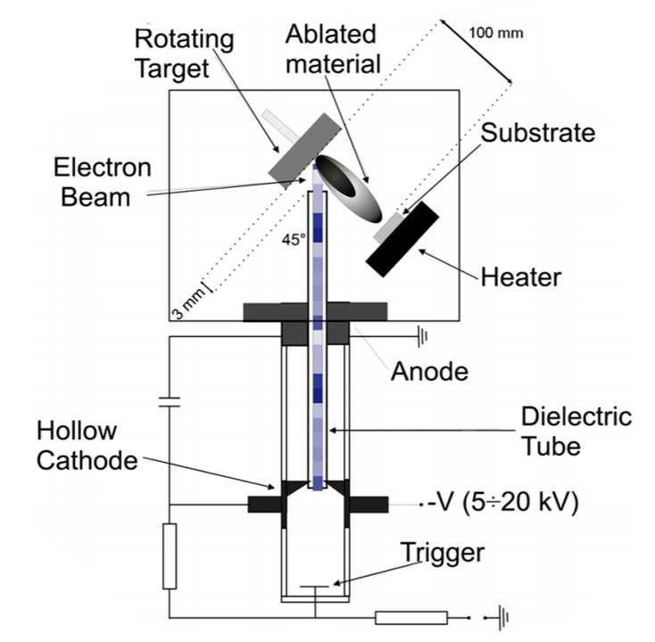
The Low-Temperature Pulsed Electron Deposition (LTPED) deposition technique is a new vacuum technology for thin films developed by CNR-IMEM for the low temperature growth of cells and photovoltaic modules on a wide range of substrates. The LTPED deposition chambers used for the production of solar cells in the laboratory have been designed and developed by CNR-IMEM. A typical LTPED cannon operates at a pressure of ~ 10-3 mbar to form a plasma cloud. At the end of the gun, a few centimeters away, there is a support designed to accommodate one or more circular targets with a diameter of 1 or 2 inches and a thickness of a few mm. Each target is a slice of the material to be deposited obtained from an ingot or preformed by sintering techniques. The material to be deposited on a special substrate which can be plastic, glassy or metallic is extracted from the target. In principle, photovoltaic thin films can be deposited using a wide range of different techniques. In the case of CuInGaSe2 (CIGS), the basic material of our solar cells, co-evaporation and sputtering are currently used in industrial production processes. What makes the LTPED process unique compared to alternative technologies is the fact that it operates far from the thermodynamic equilibrium. Because of this, thin films of materials with a very complex phase diagram, such as CIGS or YBCO, can be obtained in vacuum without the need for high pressure or high temperature post-deposition treatments which also involve toxic gases. The main component of a pulsed electron deposition system is the source of the electron beam. Our research equipment is based on Neocera PEBS-20 pulsed electron sources mounted at about 45° with respect to the target support and operates at a discharge voltage between 12 kV and 18 kV with an activated pulse repetition frequency of 10 Hz. The targets are positioned just below the electron sources, while the solar cell substrates are mounted upside down on a horizontal sampling stand facing the target surface. During the deposition process, argon is introduced into the chamber to allow the generation of the electron beam and its effective propagation towards the target. A successful CIGS photovoltaic quality deposition is obtained by tuning the deposition parameters in order to optimize the target ablation and minimize any secondary evaporation effect. Further details on the LTPED process and on the characteristics of the CIGS test cells manufactured with this technology can be found in this contribution. The following video is an overview of LTPED technology and its application for laboratory scale CIGS solar cell fabrication.