


Aim of the Training Network
Nanotechnology based on semiconductor nanowires promises a new generation of devices benefiting from large surface to volume ratios, small active volumes, quantum confinement effects and integration in complex architectures on the nanoscale. The main technological issues that the joint research programme intends to address within the project are the following: semiconductor nanowires for sensors, optoel-ectronic, nanoelectronic and energy harvesting applications.
The main objective of the proposed network is to embed a pool of postgraduates and young researchers in a multidisciplinary framework of research and development activities in the emerging field of science and applications based on the unique properties and opportunities offered by semiconductor nanowires. Our mission will be to provide an excellent platform for the training of a generation that will be expected to play a leading role in developing new ideas and concepts for a truly new technology of the future. Attainment of our targets will make a substantial contribution to increased European competitiveness in one of the most important emerging technological fields.
The integration of two leading companies as full partners in the ITN underlines the strategic importance of the proposed research subject and approach. The active participation of the private sector gives additional value to the training of the early state researchers. Moreover, the synergy between partners from academia and from the private sector will contribute to expedite the research activities in Europe towards a market maturity of nanowire based applications. The project started officially on 01. November 2010 with a duration of 4 years.
Research overview
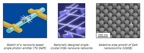
The interest in bottom-up fabricated semiconductor nanowires has been growing steadily in the last years due to their potential as basic building blocks of nanoscale devices and circuits. Investigations performed so far try to exploit three unique properties of nanowires: First, they are the smallest dimension structures that allow optical guiding and electrical contacting simultaneously. Second, their large surface to volume ratio enhances their interaction with the environment, turning them into optimal chemical and biological sensors. Finally, their anisotropic geometry makes their optical and electrical properties dramatically dependent on their orientation, allowing their use as polarization-dependent sensors.
Most nanowire applications rely on the ability to grow, characterize (structurally, optically and electronically) and manipulate both individual and collections of nanowires. To date it is rather difficult to find a single research group covering all of the above competences, and students usually focus on a single aspect of nanowire-based device realization (either growth, characterization, simulation or device assembly). The scope of this project is to create a European Network of experienced teams that will provide early stage researchers with a multidisciplinary framework and a comprehensive training in the field of nanowire physics and applications. The active involvement of industrial partners will ensure that the acquired competences are driven by industrial needs, such as scalable and low cost nanowire production. The interaction with associated industrial partners will also add to the employability of the recruited researchers through the exposure to the private sector.
The main applications that we intend to address within the project time are the following:
- Nanowires for sensing applications
- Nanowires for optoelectronics
- Nanowires for nanoelectronics
- Nanowires for energy harvesting
Project partners
Full Network Partners
Georg-August-Universität Göttingen (Germany) - Angela Rizzi (Coordinator), Joerg Malindretos
Friedrich-Schiller-Universität Jena (Germany) - Carsten Ronning
Universitat de Valencia (Spain) - Nuria Garro
Installation Europeenne de Rayonnement Synchrotron (France) - Gema Martinez-Criado
University of Cambridge (United Kingdom) - Richard Phillips
University College Cork, National University of Ireland (Ireland) - Daniela Iacopino
Technische Universiteit Delft (Netherlands) - Leo Kouwenhoven, Val Zwiller
Hochschule RheinMain (Germany) - Michael Indlekofer
Consiglio Nazionale delle Ricerche (Italy) - Giancarlo Cicero, Alessandra Catellani
Centro Ricerche FIAT S.c.P.A. (Italy) - Daniele Pullini, Gianfranco Innocenti
AIXTRON SE (Germany) - Michael Heuken, Christoph Giesen
Technische Universiteit Eindhoven (Netherlands) - Erik Bakkers
Associated Partners
CIDETE INGENIEROS SL (Spain)
Institut für Solarenergieforschung GmbH (Germany)
University of South Florida (USA)
LPE S.p.A - Epitaxial Technology /
ETC SRL - Epitaxial Technology Center (Italy)
Vishay Semiconductor Italiana S.p.A (Italy)