


The research activities of this AdR are conducted at four research laboratories within IMEM and research facilities at INRiM-PiQuET, Chi-Lab/DISAT at Polytechnic University of Turin, and the Department of Chemical Science and Technology at the University of Tor Vergata.
FABRICATION AND CHARACTERIZATION OF THIN FILMS
The laboratory is equipped for the synthesis of innovative materials of natural and/or synthetic origin and for the deposition of polymeric thin films using various techniques:
Langmuir Schaefer and Langmuir Blodgett (KSV 5000, Nordtest)
Spin coating (Laurell)
Layer-by-Layer for polyelectrolyte multilayers
Dip coating
Electrodeposition
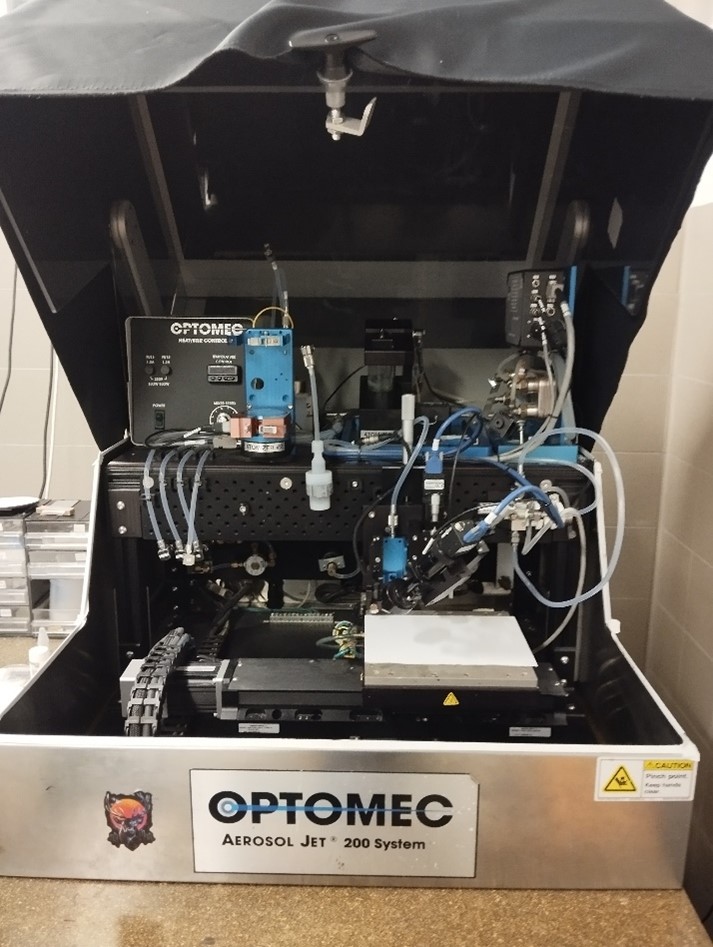
A Direct Writing system operating in non-contact mode (Aerosol Jet Printer AJ200-OPTOMEC) is available for rapid prototyping of bioelectronic interfaces and devices based on liquid-phase conductors (pictured) (both commercial and homemade inks), ensuring biocompatibility and sustainability through "green chemistry" approaches.
The laboratory features a coating system for protective coatings, flexible and freestanding substrate production, and encapsulation of devices in Parylene (Diener P6).

Diener P6

custom 3D printing system
At the IMEM facility, a custom 3D printing system is set up with six extruders for filament deposition (including two titanium extrusion heads capable of up to 400°C), pastes, and liquids with variable viscosity. The system is integrated into a biological hood for sterilization and includes
A temperature-controlled print bed with a broad range and high ramp speed
A UV laser for photo-crosslinking
A microscope for real-time monitoring of fabrication processes
A Laser Cutter is available, along with a sputtering deposition system for metals (Au for pads and electrical interconnections, Ti for adhesion layers).
UltiMaker S5 Printer for producing technical artifacts supporting research activities
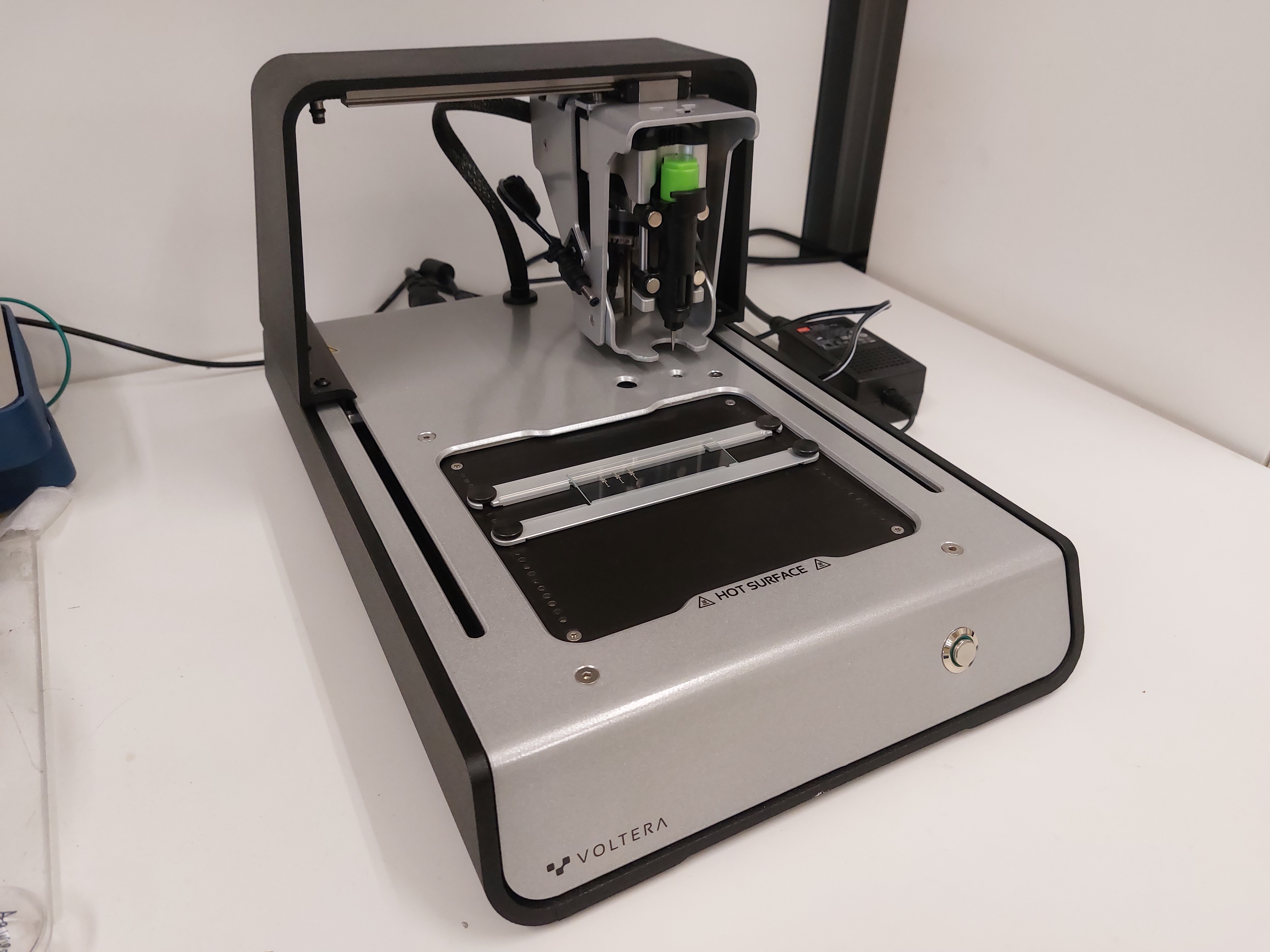
PCB Printer (Voltera) for manufacturing small printed circuits by controlled deposition of conductive inks and solder pastes on flexible and rigid substrates.
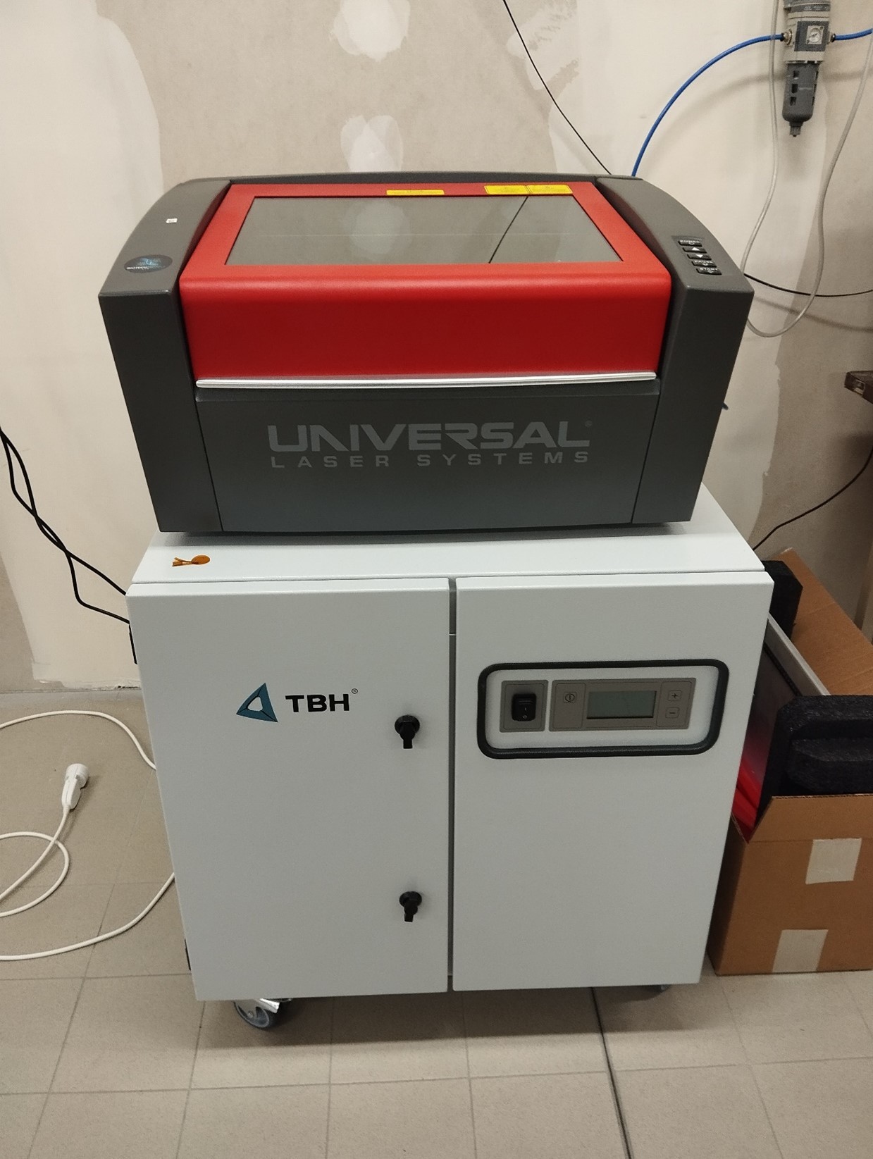
Laser Cutter
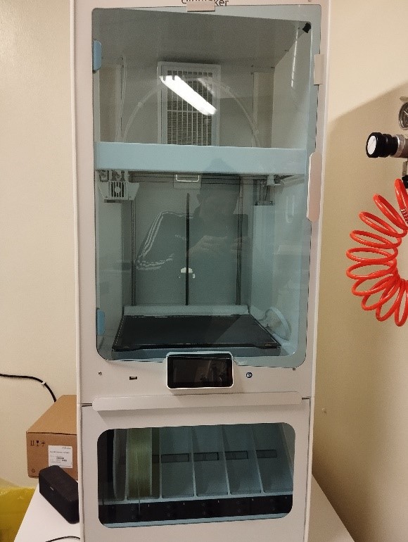
UltiMaker Printer
PCB Printer
ADDITIONAL LABORATORY EQUIPMENT:
Class 3 chemical hood
Thermal UV-Ozone Cleaner System (Novascan)
Immersion sonicator (Hielscher UP2000St)
Type 2 water purification system (Sartorius) coupled with a Milli-Q system for Type 1 water production
Infusion systems (KDS 130 Legato)
Benchtop centrifuge (Eppendorf MiniSpin)
pH meter, hot plates, ultrasonic sonicator
CHEMICAL-PHYSICAL ANALYSIS:
Our laboratories are equipped with instrumentation for the chemical-physical characterization of materials and assemblies:
ATR-FTIR (Cary 630) for spectroscopic characterization of natural and synthetic composite materials and surface functionalization monitoring
DSL Nanotrac Flex with fiber optic probe for real-time nanosystem assembly monitoring
Fluorimeter (Tecan Infinite 200 pro), plate reader with an integrated spectrophotometer
Access to UV-VIS spectrophotometry (Jasco V-770)
FABRICATION OF 3D MICRO/NANO-ENGINEERED SYSTEMS
Through collaboration with Politecnico di Torino, a cleanroom facility is available at the IMEM@PoliTo Unit for implementing micro- and nanoscale technological processes. The cleanroom consists of ISO 14644 Class 5 (U.S. Fed-Std 209D Class 100) and ISO 14644 Class 6 (U.S. Fed-Std 209D Class 1000) areas and hosts key micro-nano technologies for MEMS, microsensor, and microfluidic fabrication, as well as their integration with nanostructures:
Double side Mask Aligner
Laser Direct Writer
Reactive Ion Etcher (RIE) and Deep Reactive Ion Etcher (DRIE)
Chemical Benches for Lithographic processes and for Wet Etching
E-Gun Evaporator
Rapid Thermal Annealer (RTA)
ICP-Plasma Enhanced Chemical Vapor Deposition (ICP-PECVD)
Graphene deposition furnace
Electroplating
Hot Embossing
CNC Milling
Micro Electro-Discharge Machining.
The laboratory is also equipped with a significant set of rapid prototyping and additive manufacturing technologies:
Ink-Jet 3D Printing
3D Plastic Sintering
MicroStereoLithography
Electrospinning
Ink-Jet Printing
2 Photon Polymerization (2PP)
ELECTRONIC AND OPTICAL CHARACTERIZATION
For electrical and optical characterization, the laboratory is equipped with:
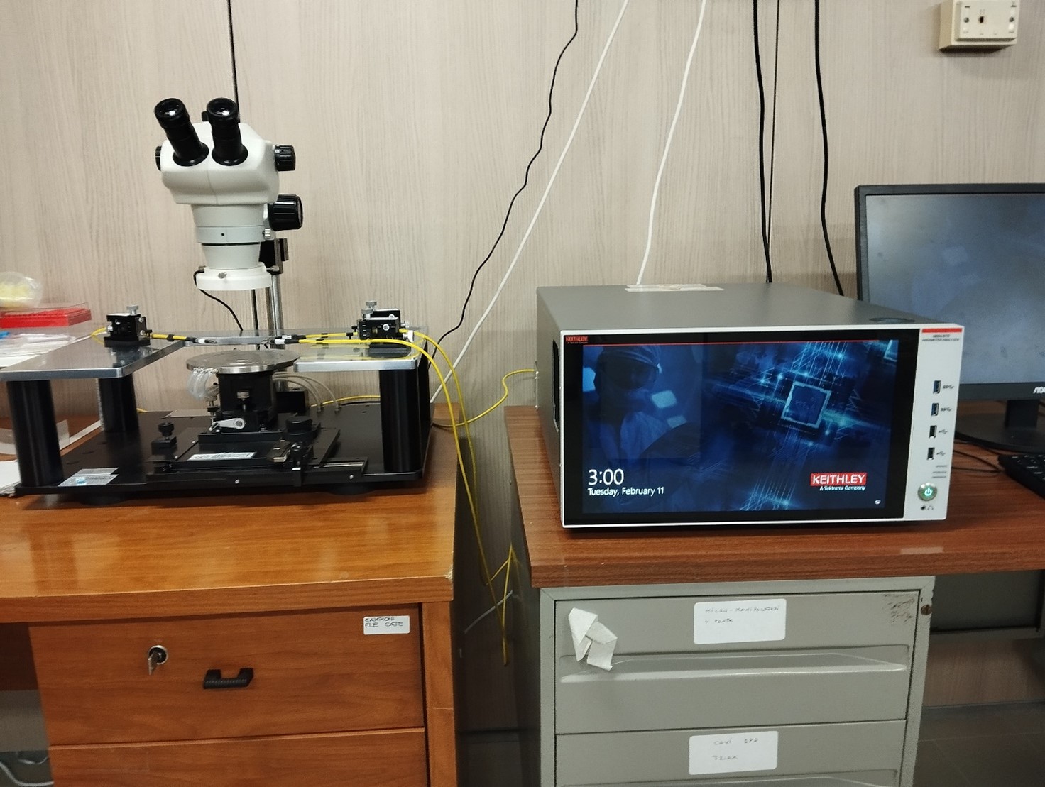
Semiconductor Parameter Analyzer (Keithley 4200) coupled with a probe station (Everbeing) for electrical response characterization of fabricated devices
National Instruments Measurement System (Chassis Ni PXIe-1073; Modules: SMU NiPXIe 4138/39, NiPXIe-6289) for electrical characterization of single electronic devices or integrated circuits .
VersaSTAT 3 Potentiostat for electrochemical measurements and interface characterization
Palmsens4 Portable Potentiostat for "on-field" measurements
Digital Oscilloscope (Tektronix 4 series)
Two DAQ data acquisition systems (Keithley Daq6510) located in a biological hood for studying biosystem activity
Electrometers (Agilent B2902A SMU dual-channel, two Keithley 2400)
A fully motorized NIKON-ECLIPSE Ni-E optical microscope
 quipped with a DS-Qi2 camera and epifluorescence setup is available. This system is primarily used for sample inspection, including topographic imaging (Z-stack) and large-scale imaging (Large Image), as well as biological sample analysis in reflection, transmission, and epifluorescence modes at various wavelengths (λ-stack).
Additionally, the laboratory has access to a FIB-SEM (Auriga Compact, Karl Zeiss) equipped with an EDX module for structural analysis.
Finally, the lab provides a small facility for the prototyping and programming of interactive systems (sensor + actuator) using various Arduino boards.