IMEM collaborates with the European Synchrotron Radiation Facility (ESRF) for the realization of pixelated detector based on CdZnTe (CZT) for imaging purposes. ESRF and others important research facilities are investigating high-Z materials to replace the current detection systems based on silicon which are limited by a low efficiency above 20 keV. The electric properties and homogeneity of CdZnTe crystals make the realization of large area devices (> 1 cm2) with a fine spatial resolution (< 100 µm) and optimal energetic resolution a challenging goal.

The role of IMEM in this collaboration concerns several aspects of this project.
- Study of the material.
IMEM is evaluating different CdZnTe crystals, both commercial ones and self-made ones (grown at IMEM with the Boron Oxide Encapsulated Vertical Bridgman technique). Detectors have been realized with such different materials in order to compare their performance and to define the best candidate.
- Electrode patterning.
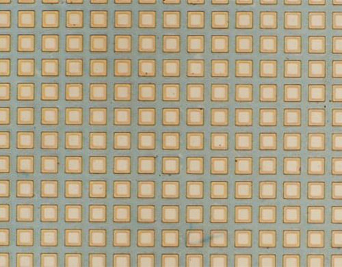
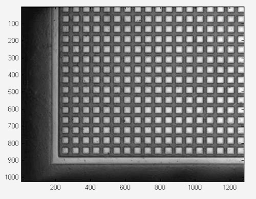
The fabricated detectors have a pitch of 55 μm and 75 μm. While this spatial resolution is easily achievable on silicon, it is extremely challenging on CdZnTe. The surface preparation (lapping/polishing), the contact deposition and the photolithographic patterning must be finely tuned in order to obtain good and reproducible results. IMEM developed a specific fabrication procedure to obtain such detectors, in collaboration with due2lab srl.
- Crystal and detector characterization.
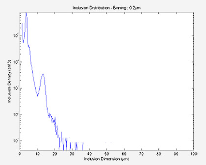
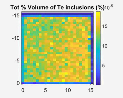
IMEM can perform different characterizations before, during and after the realization of the sensors to ensure a good final quality. Crystals have been inspected with Infrared Microscopy technique in order to quantify the concentration and distribution of defects (dislocations, tellurium inclusions) in the starting material. The quality of the surfaces before and after contact deposition has been checked through optical inspection. Finally, current/voltage behaviour of the final detectors has been measured..
