


Nowadays ionizing radiation detectors are widely employed in several application fields. These include medical imaging (CT, SPECT), environmental monitoring (control of the background radiation and contaminated areas), homeland security (cargo and luggage control), industrial controls (material quality and/or foreign bodie checks) and astrophysics (study of X- and gamma-ray emission from celestial bodies).

In last decades the use of semiconductor devices is getting more and more important in these fields and they have replaced classical scintillators in various application. Semiconductor based detectors can achieve better energy resolution thanks to the direct conversion of incident radiation into electrical signal. In addition semiconductor materials, compared to scintillators, allow to achieve higher spatial resolution in imaging detectors. These characteristics make semiconductors the most advanced technology for radiation detection of X- and gamma-photons in the energy range betweeen 1 keV and 10 MeV.
Taking into account the key demands of radiation detector applications, several semiconductor materials have been studied after that year . The main requests for such materials are: I) high stopping power even for energetic radiations; II) spectroscopic capability; III) imaging capability with good spatial resolution; IV) possibility to operate at room temperature; V) excellent mechanical rigidity to fabricate compact and stable systems.
IMEM and CdZnTe (CTZ)
Among the compound semiconductors, Cadmium Zinc Telluride (CdZnTe or simply CZT) is one of the few materials that fulfills all the requirements listed above. CdZnTe represents the best compromise in terms of energy efficiency, high atomic number, resistivity, and room temperature operation capability.
In particular, its attractive characteristics are:
- Bandgap of 1.57eV, that is at the same time wide enough to make high resistivity possible and narrow enough to ensure low pair-production energy (high signal-to-noise ratio).
- Mean atomic number of 50, which means a good stopping power also for high-energy radiation.
- Electron mobility-lifetime product sufficiently high.
- Possibility to growth large single crystals.
For all these reasons CZT is today considered the ideal material to make this kind of devices.
CZT and the detectors made with this material have been studied at IMEM for more than 20 years and actually our Insitute has active collaboration with several national and international research groups and companies working in this field.
IMEM's expertise in CZT and X/Gamma ray detectors extends over several different aspects:
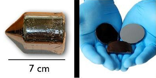
1. Crystal growth
A Vertical Bridgman furnace is present at IMEM laboratories. Thanks to the long time experience in this field, we can growth now large and state-of-the-art CZT single crystals with competitive transport properties and extraordinarily high resistivity.
The use of single crystals is essential for this kind of applications. Polycrystalline material, indeed, generally has poor transport properties becuase of charge carriers recombinations at grain boundaries. In the case of CZT, the production of single crystals with large dimension and ideal physical properties is absolutely not trivial. CZT crystals are obtained starting from very high purity precursors, avoiding most of contaminations during all the growth steps and optimizing the growth procedure.
Today, the two growth techniques that are most widely used for CZT are Traveling Heater Method (THM) and Bridgman (high-pressure, low-pressure, and boron-encapsulated).
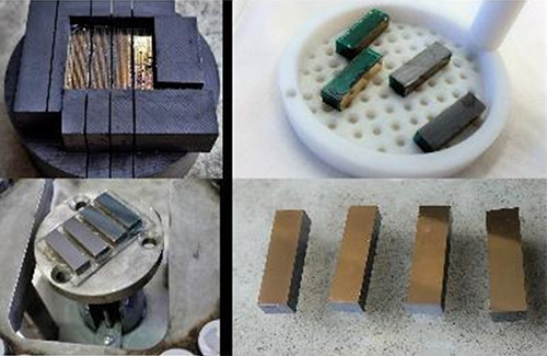
2. Detectors fabrication
Detectors can be fully fabricated in IMEM. Fabrication process starts with the material selection (self-produced or commercial CZT) and ends with bonding on dedicated boards passing through lapping, polishing, contact deposition and passivation.
An accurate selection of material is needed to obtain detector with good transport properties and consequently high performances. Because of risk of crystal damaging or cracking, cutting process is critical and special precautions are used, especially when small CZT blocks are needed. The following step is surface preparation on which contacts are deposited: they must be homogenous, with low roughness and not-oxidized. A meticulous two-step process of lapping and polishing is required to reduce roughness; this process leaves surfaces very clean and ready for contact deposition. The available contacts depositions are different and depends on the detector characteristics: Au and Pt ca be evaporated, but also deposited by room-temperature electroless technique (Ni contacts are also deposited in this way).
The clean room present in our institute allows the realization of customized contact patterns. Passivation is, generally, the last process of sample realization, strongly reducing the leakage current that flows between different contacts (sometimes over three degree of magnitude).
Thanks to decades of experience we are today among the worldwide leaders in custom detector fabrication and several international research groups keep asking us to realize customized detectors, like for example those for ESRF and ASI projects.
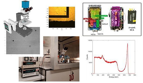
3. 3. Material and detectors characterization
IMEM has facilities to characterize the both raw material (IR scan for Te-inclusion detection, optical microscope) and the realized detectors (probe station for electric characterization, readout electronic chain and radioactive sources).
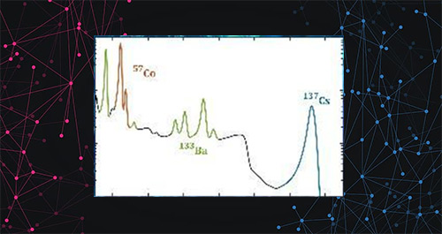
IMEM has facilities to characterize the both raw material (IR scan for Te-inclusion detection, optical microscope) and the realized detectors (probe station for electric characterization, readout electronic chain and radioactive sources). Te-inclusions severely limit the performances of CZT-based detectors, particularly in the case of imaging sensors. Hence, monitoring tellurium inclusion density and distribution is very important for assessing the material quality, for studying the formation mechanisms and for checking the effectiveness of post-growth thermal treatments used to reduce inclusion concentration. An ad-hoc system for 3D reconstruction of inclusion distribution based on optical microscopy was developed in IMEM. It allows to scan from small CZT blocks to entire wafers, with a minimum inclusion size of few microns. Electric characterization of sensors, instead, is fundamental because it provides important information on the detector characteristics and its working performance as radiation detector. Then, the realized sensors can be tested for spectroscopic response with standard nuclear sources (241Am, 47Co and 137Cs).
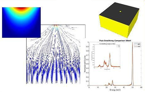
4. Simulation of detector response and spectral correction
The simulation tool developed in our institute ca model all the physical processes involved in the formation of the detector signal, from the radiation absorption mechanisms to the influence of the electrodes geometry.
The simulation system is based on first principle calculations and consists in a Monte Carlo simulator, a Finite Elements Method (FEM) calculator and numerical computation software. Radiation–semiconductor interaction, charge carrier transport, role of the electric field, and weighting field in signal induction on the electrodes are simulated. It is possible to simulate the entire experimental arrangement including the use of attenuators, collimators and scattering surfaces. This simulator is used to develop corrective algorithm to remove spectral distortions which intrinsically affect this type of sensors.
5. Isotope identification
IMEM started dealing with algorithms able to find the radionuclides present in a measured gamma spectrum. Thanks to a machine learning approach, IMEM developed an algorithm able to identify isotopes in extremely noisy spectra with great accuracy.
IMEM started dealing with algorithms able to find the radionuclides present in a measured gamma spectrum. Thanks to a machine learning approach, IMEM developed an algorithm able to identify isotopes in extremely noisy spectra with great accuracy.
Collaborations
In the last years IMEM established collaborations with several international research laboratories and leading companies of this field.
Main active collaborations are:
- Rutherford Appleton Laboratory (RAL, Oxfordshire, UK). Here advanced ASIC readout electronics are realized; several CZT sensors realized by IMEM were bounded on this ASIC and measured at the Diamond Light Source synchrotron at RAL.
- University of Parma (UNIPR, IT), Physics Department. An advanced facility to perform laser induced transient current technique and nuclear sources, necessary to characterize detectors, are available here.
- University of Palermo (UNIPA, IT), Physics Department. Worldwide experts in digital electronics for detectors; digital approach has a key role to increase the performances of these devices. Both spatial and energy resolution can be increase thanks to it.
- INAF di Bologna (IT). Here researchers deal with instrumentation for hard X and soft gamma ray astronomy and CZT for astrophysics applications. Large volume 3D detectors are studied in order to track Compton event and recognise radiation sources in deep space.
- INFN Pavia (IT). Boron Neutron Capture Terapy (BNCT) is studied here. This is an experimental adrotherapy for treating locally invasive malignant tumours and it is based on neutron irradiation of enriched cancer. Alpha particle and gamma photon are generated after neutron capture by 10B atoms; alpha particle kills cancer cell while, due to its high penetrating power, gamma photon escape away from the body and can be detected to monitor the therapy. To distinguish these photons in the zoo of ionizing particles presents during the therapy is not easy. CZT detectors are used for this task.
- XNEXT s.r.l. (Milano, IT). An intensive knowledge scale-up company, that produces and develops the most advanced X-ray spectroscopic technology available today to perform in-line real-time identification. Several research contracts has been stipulated between XNEXT and IMEM with the purpose of investigate different CdTe and CZT materials and develop innovative algorithms concerning the field of spectral correction and pileup suppression.
- European Synchrotron Radiation Facility (ESRF, Grenoble FR). ESRF and others important research facilities are investigating high-Z materials to replace the current detection systems based on silicon which are limited by a low efficiency above 20 keV. IMEM collaborates with the European Synchrotron Radiation Facility (ESRF) for the realization of pixelated detector based on CdZnTe for imaging purposes.
Projects
Main active projects related to CZT and CTZ-based detectors are::
- Astra: Advanced ultra-fast solid state detectors for high precision radiation spectroscopy (STRONG, European Project)
- 3DCZT Module (3DCaTM) for spectroscopic imaging, timing and polarimetry in hard X-/ soft γ-rays satellite mission (ASI/INAF)
- Development and characterization of linear array of detector for X-ray scanner (research contract with Xnext)
- CZT pixelated sensors (contratto di ricerca con European Synchrotron Radiation Facility, ESRF)
Applications
CZT characteristics allow it to be employed in a number of different application fields:
- Environmental monitoring
Techniques to detect Radiological and Nuclear (RN) agents are strongly requested in the field of homeland security (border and port security) and environmental monitoring, for the rapid scanning of sensitive areas (restaurants, airports, subway stations, shopping malls, etc.) that are possible targets for terroristic threats like dirty bombs or silent sources. Thus, the development of smart radiation detectors that detect, measure, identify and analyse gamma ray emitting radioactive sources is a primary need. [read more...] - Non-destructive testing
The penetrating power of high energy photons led to the realization of new inspection techniques able to literally “see” inside an object without breaking or opening it. This process is called “non-destructive testing” (NDT) and represented a breakthrough in industry since it allowed to rapidly verify the quality and to detect the presence of contaminants in the final industrial product. [read more...] - Astrophysics
The capability of detecting this type of light has a crucial role in the observation of celestial bodies and cosmic radiation. In fact, the light coming from space covers the whole electromagnetic spectrum and, thus, its measurement in the keV to MeV energy band is essential to complete the picture. [read more...] - Medical imaging
The use of solid state devices rejects in the production of new medical devices, with far higher performances with respect to scintillators or other devices. SPECT (Single Photon Emission Computed Tomography) or CT (Computed Tomography) are techniques that are becoming more and more common in the preventative medicine or surgical applications and the use of such devices have been a great help in the cure and detection of diseases. - Imaging
ESRF and others important research facilities are investigating high-Z materials to replace the current detection systems based on silicon which are limited by a low efficiency above 20 keV. The electric properties and homogeneity of CdZnTe crystals make the realization of large area devices (> 1 cm2) with a fine spatial resolution (< 100 µm) and optimal energetic resolution a challenging goal. [read more...]