


The applications of X- and gamma-rays detectors span several fields from specific research topics (e.g., astrophysics, fundamental physics) to more practical sectors related to the everydays life (inspection of industrial products, security controls).
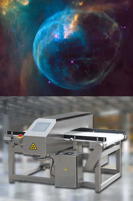
In the former case, the capability of detecting this type of light has a crucial role in the observation of celestial bodies and cosmic radiation. In fact, the light coming from space covers the whole electromagnetic spectrum and, thus, its measurement in the keV to MeV energy band is essential to complete the picture. In the latter case, the penetrating power of high energy photons led to the realization of new inspection techniques able to literally “see” inside an object without breaking or opening it. This process is called “non-destructive testing” (NDT) and represented a breakthrough in industry since it allowed to rapidly verify the quality and to detect the presence of contaminants in the final industrial product.
IMEM is active since several years in both these sectors thanks to its CZT-based detectors.
Industry: non-destructive analysis
Nowadays, X-ray inspections are employed in several industrial applications (e.g. food and pharmaceutical products inspection, in-line density control). Depending on the thickness, density and composition of the object that must be inspected, the intensity and energy of the artificial radiation source (a X-ray tube) can be very different. As a consequence, the X-ray detection systems must be adaptable to different operating conditions in terms of radiation flux and energy and to different inspected objects in terms of shape and dimension. At the same time, spatial and energy resolutions must be adequate to the dimension and composition (defect, impurities, contaminants).
Basically, inline X-ray imaging of industrial production can be achieved by realizing linear array detectors. The sequential acquisition of 1D images allows to reconstruct the complete image of the product: if it does not satisfy certain requirements, the object is removed from the production line. Currently, standard X-ray sensors produce images by exploiting the measured intensity of the whole incoming radiation or, at most, of two energy bands. Thickness and density of the inspected materials can be estimated from this type of measurements.
On the other hand, a spectroscopic detector can produce a “coloured” image which provides information also on the chemical composition, thus allowing to distinguish two materials with similar density and thickness but with different elemental composition.
IMEM collaborates with Xnext s.r.l., an emerging italian company which produces advanced X-ray inspection systems by exploiting spectroscopic solid-state-based linear scanners. The topics of this collaboration spans from the material characterization to the detector design, up to the development of new data analysis methods (click here to read more about this project).
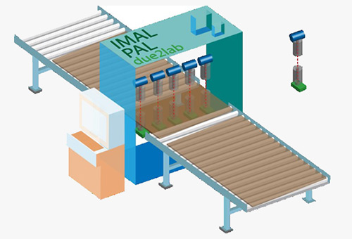
IMEM also collaborates with due2lab s.r.l. for the development of a new technology capable of gathering all the useful information contained in the X-ray spectrum and thus returning all material characteristics. This type of inspection technology differs by previously mentioned linear scanner because this is based on a larger single detector which can be used for much larger objects, like ,for example, wood panels or ceramic tiles.
Traditional X-ray NDT techniques that work in transmission mode (when the object is placed between X-ray source and detector) for density measurement is that they return a density value which is "relative". Thus a calibration procedure is necessary every time the production type is changed, and periodically if the production line is subject to small chemical composition variations of the raw material.
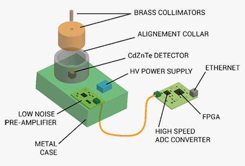
On the contrary, this CZT-based system provides real time absolute density measurements by exploiting the hyper-spectral capabilities of its detector. A schematic 3D model of realized prototype is shown in following figures (single detection unit with important parts highlighted is shown in the first image, while the complete in-line scanner is schematically represented in the second one).
Space: detection of cosmic radiation
X- and gamma-radiation detectors find application in space exploration and are essential to solve several still open hot scientific topics regarding the observation of cosmic ray sources (e.g., pulsars, black holes, binary systems). Lightness, compactness and low-power consumption are mandatory since the whole system must be suitable to be assembled on several types of satellites. Furthermore, fine energy resolution (in the order of few keV) and three dimensional position sensitivity with sub-millimeter spatial resolution are generally required.

In this context, CZT-based detectors assume an important role thanks to the density and atomic number of the material that guarantee a high stopping power. Conversely to Si- or Ge-based sensors, with CZT single photon counting capabilities are possible without requiring cooling systems. Hence, it represents the ideal candidate for this purpose.
IMEM, as one of the global leader in research of CZT-based detector, has been and is involved in projects related to astrophysical studies. IMEM expertise in fabrication and characterization of custom detectors and the collaboration with due2lab s.r.l. led to the realization of a 3D drift strip detector. This prototype can be the basic element for the realization of high performance detectors in spectroscopy, imaging, timing and polarimetry both as focal planes on space telescope implementing new high energy optics (e.g. Broadband Laue lens), and for small wide field instruments to be used in the future on clusters of micro satellites.
Collaborations with Synchrotron facilities
In the last few years, spectroscopic solid-state detectors started replacing the current standard X-ray system technologies. However, several aspects of CZT-based sensors are yet to be understood. Great scientific efforts are spent in order to improve the performance of these detectors in specific and unusual conditions, especially by large facilities like synchrotrons, by realizing focused experiments. Indeed, synchrotron light represents the best radiation source to test these devices thanks to the possibility of controlling the beam size, position, energy and intensity. IMEM-CNR collaborates with both the largest European synchrotrons: the Diamond Light Source (DLS) in Oxfordshire (UK) and the European Synchrotron Radiation Facility (ESRF) in Grenoble (France).

IMEM-CNR collaborates with a division of the STFC Rutherford Appleton Laboratory (Oxfordshire, UK) which designs, develops and tests integrated circuits for the readout of several types of sensors, including CZT-based ones for imaging purposes. The long term experience in the realization of detector of IMEM combined with the know-how on ASIC developed at RAL and the digital correction approach studied by physics department of UNIPA gives rise to a strong collaboration with the goal of studying the performance of pixelated detectors in particular conditions (e.g., photons interacting in the intergap region, effects of high fluxes). This allowed to obtain access to the DLS facility which resulted in several scientific publications and contributions to the most prestigious conferences on this topic.

IMEM collaborates with the ESRF for the realization of pixelated detector based on CdZnTe for imaging purposes. ESRF and others important research facilities are investigating high-Z materials to replace the current detection systems based on silicon which are limited by a low efficiency above 20 keV. The electric properties and homogeneity of CdZnTe crystals make the realization of large area devices (> 1 cm2) with a fine spatial resolution (< 100 µm) and optimal energetic resolution a challenging goal. The role of IMEM in this collaboration concerns several aspects of this project.i (click here for further information on this project).