


 FOR MORE INFORMATION: Marco V. Nardi - +39 0461 314849 - marcovittorio.nardi@imem.cnr.it
MoS2 thin layers with few-layer properties on large area substrates
We utilize ionized jet deposition (IJD) and annealing at 250 °C to grow MoS2 thin films in a versatile and industrially scalable way.
Even though the IJD-deposited MoS2 films are more than 100 nm thick, they remarkably display 2D electronic and optical properties: they exhibit a bandgap of 1.86 eV and well-resolved photoluminescence (PL) spectra with an excitonic linewidth of less than 10 meV. This behaviour has been obtained thanks to the encapsulation of crystalline 2D MoS2 nanosheets (single or few layers) in an amorphous MoS2 matrix (“2D-in-3D” structure).
The obtained results represent a breakthrough towards the large-scale and affordable production of 2D-like materials.
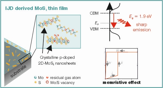
"2D-MoS2 goes 3D: transferring optoelectronic properties of 2D MoS2 to a large-area thin film" – M. Timpel et al. - npj 2D Mater. Appl. 5 (2021) 64 - https://doi.org/10.1038/s41699-021-00244-x
IJD-MoS2: Role of Substrate and Working Parameters
To investigate possible interactions of the IJD target plasma with the substrate, e.g., SiO2/Si, the interface between as-deposited MoS2 and SiO2/Si substrate was carefully investigated. The formation of an interface comprised of several silicon oxide species was observed between MoS2 and the silicon substrate, which is suggested to originate from etching and oxidizing processes of dissociated water molecules in the vacuum chamber during growth.
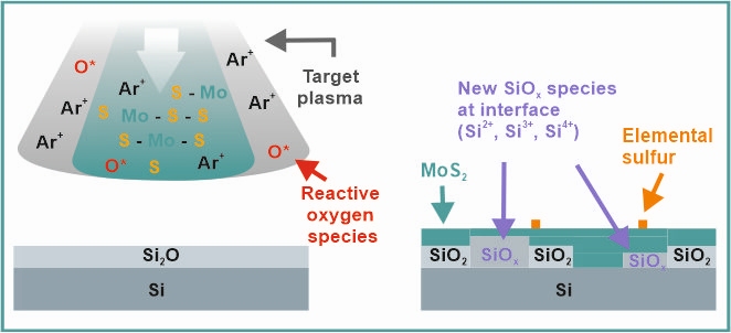
(a) before ionized jet deposition; (b) initial etching of the SiO2 native oxide; (c) formation of complex
SiOx surface and MoS2 thin film growth.
"Synthesis of MoS2 Thin Film by Ionized Jet Deposition: Role of Substrate and Working Parameters" – A. Ghiami et al. - Surfaces 3 (2020) 683 - https://doi.org/10.3390/surfaces3040045