


Materials, in the wider meaning of the word, are considered as the starting point to develop novel applications, to explore new science and to foster collaborations.
This research activity is devoted to the growth and synthesis of nano-, low-dimensional (1D, 2D) and functional materials, thin films and bulk compounds using the different techniques available at our institute.
We are involved in the growth and synthesis of:
- Nanomaterials (semiconductors and oxides)
- Low-dimensional (1D, 2D) and functional materials
- Thin films and bulk compounds
The main topics of our research activities are:
|
|
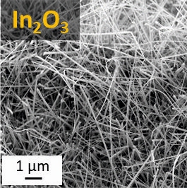
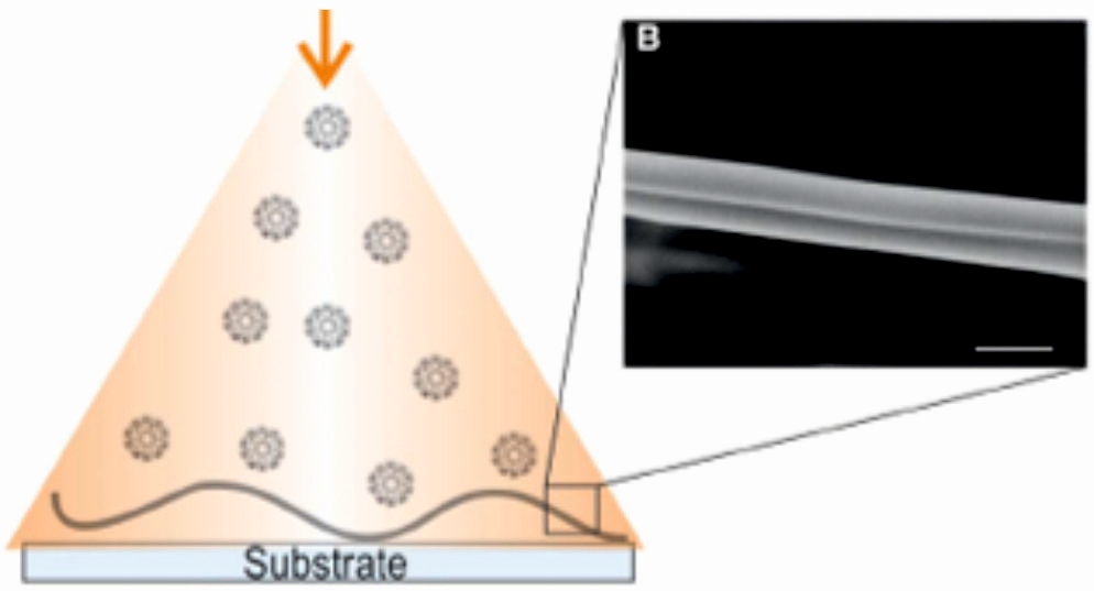
Nanostructures and nanosystems: low dimensional structures such as nanowires, nanorod and nanopods of different compounds (e.g. oxide, elemental semiconductors) are synthesized by different techniques (solution, vapor, CVD) and used for applications such as gas sensing or energy harvesting. [...] |
|
|
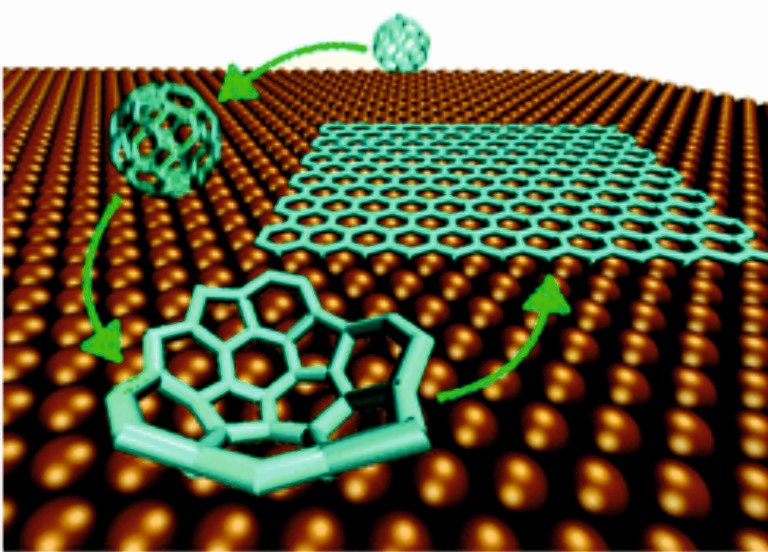
2D materials: graphene and transition metal dichalcogenides (TMD, e.g. MoS2) are the playground for new science and new applications such as gas detection and optical sensing. Functionalization of graphene and TMD and the study of their defects allows to extend the possibility of applications and to understand the relationships between the atomic structure and the functionality of these materials. [...] |
|
|
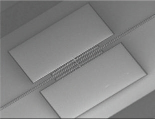
Thin films and bulk crystals: Bridgman growth and synthesis from melt at high T of ingots of different materials are used to produce X-Ray detectors, targets for film deposition and source materials for bulk single-crystal growths. Thin films for sensing and power devices are realized by MOVPE, while magnetic materials and intermetallic compounds are obtained with RF sputtering and arc-metlting. Pulsed Electron Depostion of complex materials permits to preserve the stoichiometry of the ablated target, to realize novel thin film CIGS solar cells. [...] |
|
|
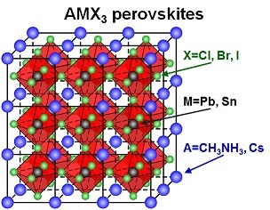
Soft matters and hybrid materials: Preparation of metal halide perovskites by solution methods and/or Single Source Thermal Ablation. Growth of thin films of organic semiconductors with high control on the morphology and structural order via supersonic molecular beam deposition. Surface functionalization with organic (bio-)molecules via kinetic activation. [...] |
 |
The expertise of IMEM researchers in material science allows also to explore the synthesis of new materials, to develop novel growth techniques and to tailor the existing ones to specific processes. [...] |