


|
|
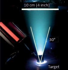
PED (Pulsed Electron Deposition) works with a high energy electronic beam to deposit the material extracted from a target onto a substrate. The beam is obtained by generating a plasma in a process gas (Ar, N2, O2) thanks to the applied potential difference of 10KV. The targets are typically made ad hoc in our laboratories.
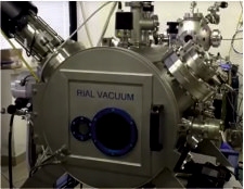
In our laboratories there are three Neocera commercial sources, installed in vacuum chambers that allow a wide variety of uses (fixed, mobile, flexible substrates, with and without heater). [...] |
|
|
IJD (Ionized Jet Deposition): this technique is very similar to PED, with a high energy pulsed electron beam inducing an ablation process on a target and enabling thin film deposition. Differently from PED, the electron beam source exploits a different technology (Noivion): a supersonic beam (Ar) is ionized to generate the main electron pulse close to the target. This leads to higher power for ablation, higher deposition rate and a high potential for industrial scalability. [...] |
|
|
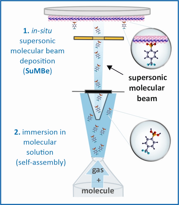
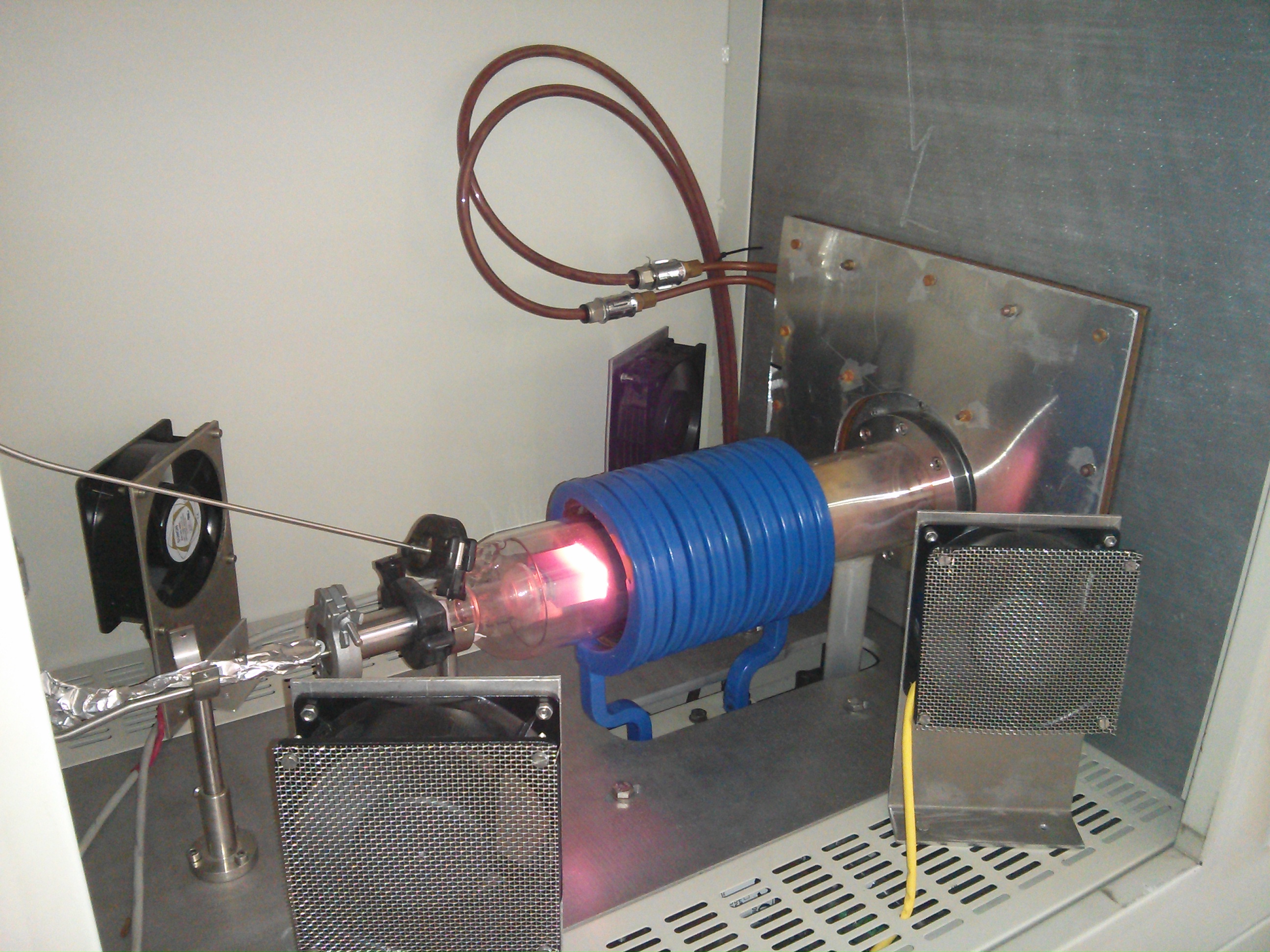
SuMBD (Supersonic Molecular Beam Deposition) is based on the seeding of heavier species inside a lighter carrier gas. A supersonic expansion is realized through a nozzle. In this way, the supersonic expansion of the lighter carrier gas determines the properties in term of kinetic energy and cooling of the heavier species. [...] |
|
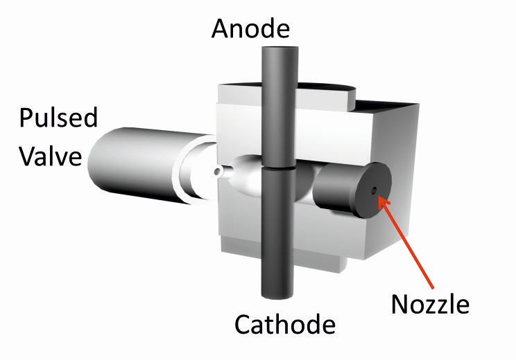
PMCS (Pulsed Microsplasma Cluster Source) is based on a pulsed source and an electrical discharge between two metallic electrodes. The gas entering in the source chamber is ionized for the discharge spattering the cathode. There is the formation of a plasma containing the material(s) of the cathode. The plasma is rapidly quenched by the entering gas causing a rapid condensation of the material with an initial cluster formation. [...] |
|
|
MOVPE (Metal Organic Vapor Phase Epitaxy): there are two MOVPE reactor in IMEM, devoted the vapor phase epitaxy of silicon carbide (3C-SiC) and gallium oxide (Ga2O3). The laboratory is equipped for the use of hydrogen and the reactors may be customized to tailor the process and the reagents, so that it is possible to explore the synthesis of new materials. [...] |
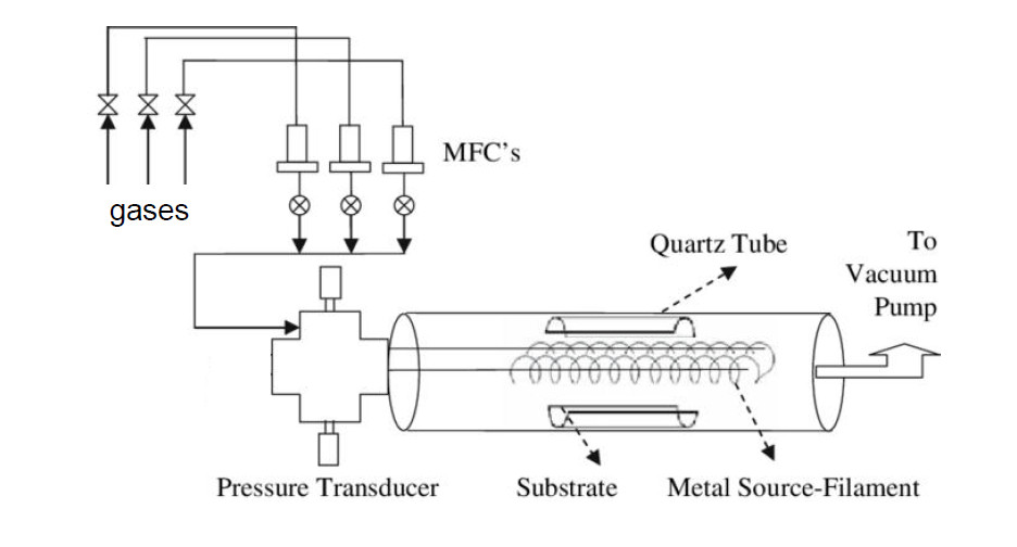 |
CVD (chemical vapor deposition): there are several reactors for the synthesis of nanostructures from the vapor phase, using the open tube method using inert gas or in oxygen. [...] |
Solvothermal process: can be defined as ‘‘a chemical reaction in a closed system in the presence of a solvent at a temperature higher than that of the boiling point of such a solvent’’. Consequently a solvothermal process involves high pressures. The selected temperature (sub- or supercritical domains) depends on the required reactions for obtaining the target-material through the involved process.