


 FOR MORE INFORMATION: Roberto Verucchi - +39 0461314825 - roberto.verucchi@imem.cnr.it
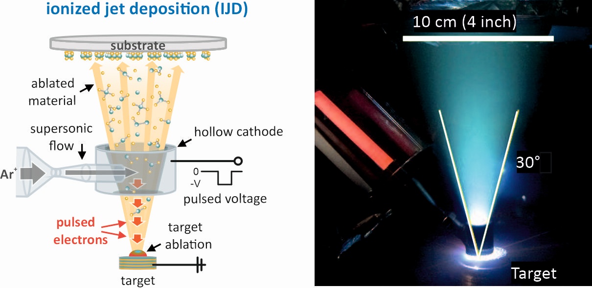
Ionized Jet Deposition (IJD) technique can produce films in vacuum, with a tunable thickness that spans from a few nm to some microns. It is based on the ablation process in a target induced by a pulsed electron beam. Likewise Pulsed Laser Deposition technique (PLD), the creation of physical vapors is due to the ablation of material induced by a large amount of energy absorbed in a defined small volume. The high temperatures achieved due to excitation of several electron levels lead to vaporization of all atoms, creating a plasma moving from the target and that can be collected on a substrate in front of it.
In PLD, energy transfer occurs from photons' absorption, with problems in non-optically active materials such as insulating materials. Moreover, high fluence, short-wavelength lasers are necessary, typically in pulsed mode, and radiation must be driven inside the vacuum chamber, where ablation occurs.
In Pulsed Electron Beam (PED) deposition technique, ablation is induced by a high energy electron pulse (about 1 J). The electron beam source is inside the vacuum chamber where deposition occurs, improving overall process reliability, and reducing cost and risks related to free photon beams in the air. However, PED is still far from being a scalable technique for industrial application due to the degradation of some source parts that require frequent maintenances.
IJD exploits electron beams, as PED, but its source has a different design to solve most of the maintenance issues and achieve higher deposited energy (up to 4J). Briefly, the main components of the IJD source and the deposition geometry are depicted in the Figure. For thin film deposition via IJD, an ionized working gas (e.g., Ar+) passes through a convergent-divergent De Laval nozzle that creates an ultrafast (supersonic) gas flow in its widening part. This ionized gas jet enters a cylinder-shaped hollow cathode, in which the electrons of the ionized gas multiply and become electrostatically confined in an equipotential space. The fast oscillation of electrons within the hollow cathode leads to an avalanche/cascade ionization of the working gas, ultimately increasing the overall ionization density by orders of magnitude (hollow cathode effect). Subsequently, high-density electron pulses are discharged with a frequency f ≤ 300 Hz (pulse length 100−300 ns) and are directed towards the grounded target (|V| ≤ 30 kV, Ipeak ≤ 6 kA with a final pulse energy E ≤ 4J). The target is composed of the material we want to deposit. The highly energetic pulsed electron beam ablates a rotating target and produces a plasma plume of ejected atomic/molecular-sized species that propagate with the working gas through the hollow cathode towards the rotating substrate. Finally, the ablated species condense on the substrate, forming a thin film over a large area (e.g., covering 5-inch wafers or larger).