


 FOR MORE INFORMATION: Marco V. Nardi - +39 0461 314849 - marcovittorio.nardi@imem.cnr.it
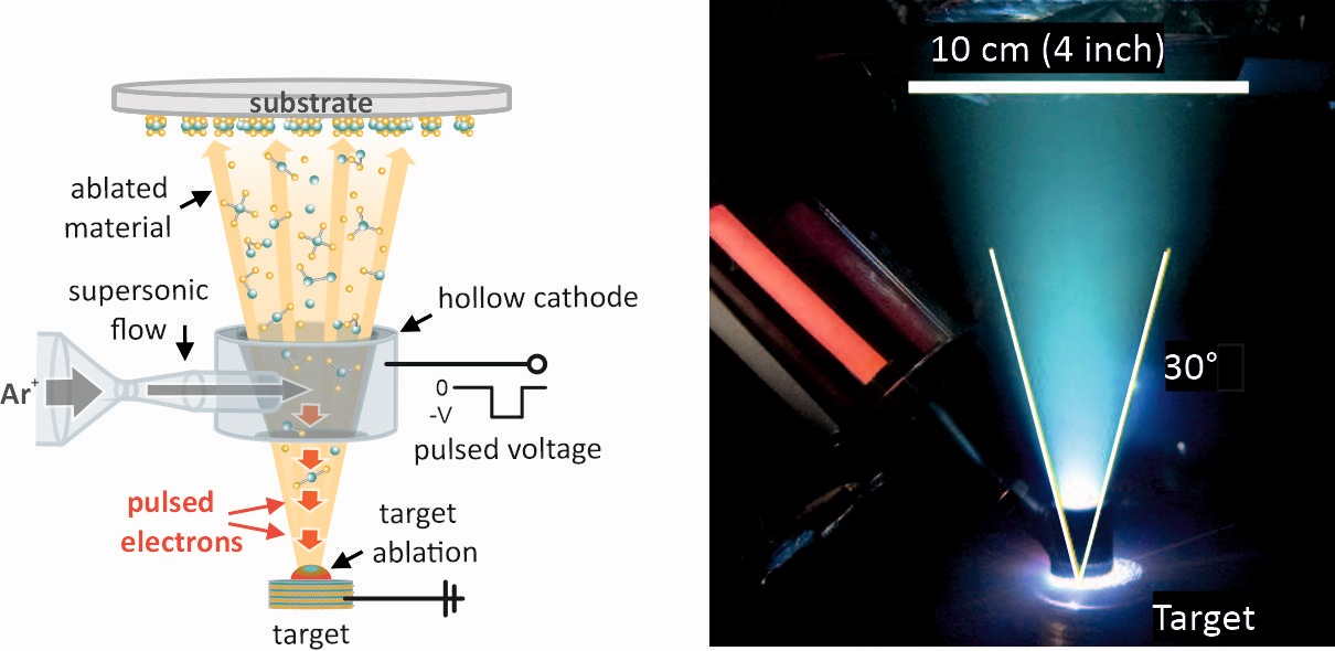
Ionized Jet Deposition (IJD) can produce films in vacuum, with a tunable thickness that spans from a few nm to some microns. It is based on the ablation process of a target induced by a pulsed electron beam. Like Pulsed Laser Deposition (PLD), the creation of physical vapors is due to the ablation of material induced by a large amount of energy absorbed in a defined small volume. The high temperatures achieved due to excitation of several electron levels lead to vaporization of all atoms, creating a plasma moving from the target and that can be collected on a substrate in front of it.
In PLD, energy transfer occurs from photons' absorption, with problems in non-optically active materials such as insulating materials. Moreover, high fluence, short-wavelength lasers are necessary, typically in pulsed mode, and radiation must be driven inside the vacuum chamber, where ablation occurs.
In Pulsed Electron Deposition (PED), ablation is induced by a high energy electron pulse (about 1 J). The electron beam source is inside the vacuum chamber where deposition occurs, improving overall process reliability, and reducing cost and risks related to free photon beams in the air. However, PED is still far from being a scalable technique for industrial application due to the degradation of some source parts that require frequent maintenances.
IJD exploits electron beams, as PED, but its source has a different design to solve most of the maintenance issues and achieve higher deposited energy (up to 4J). Briefly, the main components of the IJD source and the deposition geometry are depicted in the Figure. For thin film deposition via IJD, an ionized working gas (e.g., Ar+) passes through a convergent-divergent De Laval nozzle that creates an ultrafast (supersonic) gas flow in its widening part. This ionized gas jet enters a cylinder-shaped hollow cathode, in which the electrons of the ionized gas multiply and become electrostatically confined in an equipotential space. The fast oscillation of electrons within the hollow cathode leads to an avalanche/cascade ionization of the working gas, ultimately increasing the overall ionization density by orders of magnitude (hollow cathode effect). Subsequently, high-density electron pulses are discharged with a frequency f ≤ 300 Hz (pulse length 100−300 ns) and are directed towards the grounded target (|V| ≤ 30 kV, Ipeak ≤ 6 kA with a final pulse energy E ≤ 4J). The target is composed of the material we want to deposit. The highly energetic pulsed electron beam ablates a rotating target and produces a plasma plume of ejected atomic/molecular-sized species that propagate with the working gas through the hollow cathode towards the rotating substrate. Finally, the ablated species condense on the substrate, forming a thin film over a large area (e.g., covering 5-inch wafers or larger).
|
|
Our research activities on IJD are developed in close collaboration with Noivion S.r.l. (Italy) |
Highlights
MoS2 thin layers with few-layer properties on large area substrates
We utilize ionized jet deposition (IJD) and annealing at 250 °C to grow MoS2 thin films in a versatile and industrially scalable way.
Even though the IJD-deposited MoS2 films are more than 100 nm thick, they remarkably display 2D electronic and optical properties: they exhibit a bandgap of 1.86 eV and well-resolved photoluminescence (PL) spectra with an excitonic linewidth of less than 10 meV. This behaviour has been obtained thanks to the encapsulation of crystalline 2D MoS2 nanosheets (single or few layers) in an amorphous MoS2 matrix (“2D-in-3D” structure).
The obtained results represent a breakthrough towards the large-scale and affordable production of 2D-like materials.
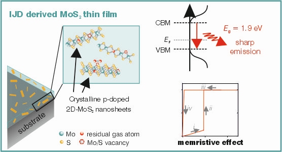
"2D-MoS2 goes 3D: transferring optoelectronic properties of 2D MoS2 to a large-area thin film" – M. Timpel et al. - npj 2D Mater. Appl. 5 (2021) 64 - https://doi.org/10.1038/s41699-021-00244-x
IJD-MoS2: Role of Substrate and Working Parameters
To investigate possible interactions of the IJD target plasma with the substrate, e.g., SiO2/Si, the interface between as-deposited MoS2 and SiO2/Si substrate was carefully investigated. The formation of an interface comprised of several silicon oxide species was observed between MoS2 and the silicon substrate, which is suggested to originate from etching and oxidizing processes of dissociated water molecules in the vacuum chamber during growth.
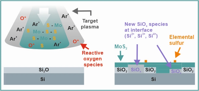
(a) before ionized jet deposition; (b) initial etching of the SiO2 native oxide; (c) formation of complex
SiOx surface and MoS2 thin film growth.
"Synthesis of MoS2 Thin Film by Ionized Jet Deposition: Role of Substrate and Working Parameters" – A. Ghiami et al. - Surfaces 3 (2020) 683 - https://doi.org/10.3390/surfaces3040045
Team members
|
|
Marco Vittorio Nardi - Researcher - Trento unit - marcovittorio.nardi@imem.cnr.it - webpage |
|
|
Melanie Timpel - Researcher - Trento unit - melanie.timpel@imem.cnr.it - webpage |
|
|
Roberto Verucchi - Researcher - Trento unit - roberto.verucchi@imem.cnr.it - webpage |
|
|
Petr Nozar - Researcher - Trento unit - petr.nozar@imem.cnr.it - webpage |