


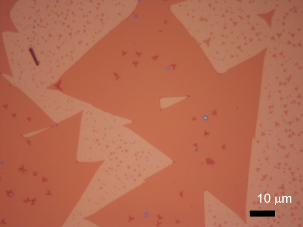
Single or double atomic layers of carbon or other atoms shows uncommon properties, often completely different from the bulk counterpart
Graphene has notable mechanical and electrical properties. However, the absence of a bandgap, typical of semiconductors, makes the realization of some devices difficult.
Transition metal dichalcogenides (TMD) such as MoS2 permit to have direct bandgap semiconductor in a form similar to graphene, permitting the integration of 2D materials to fabricate novel devices.
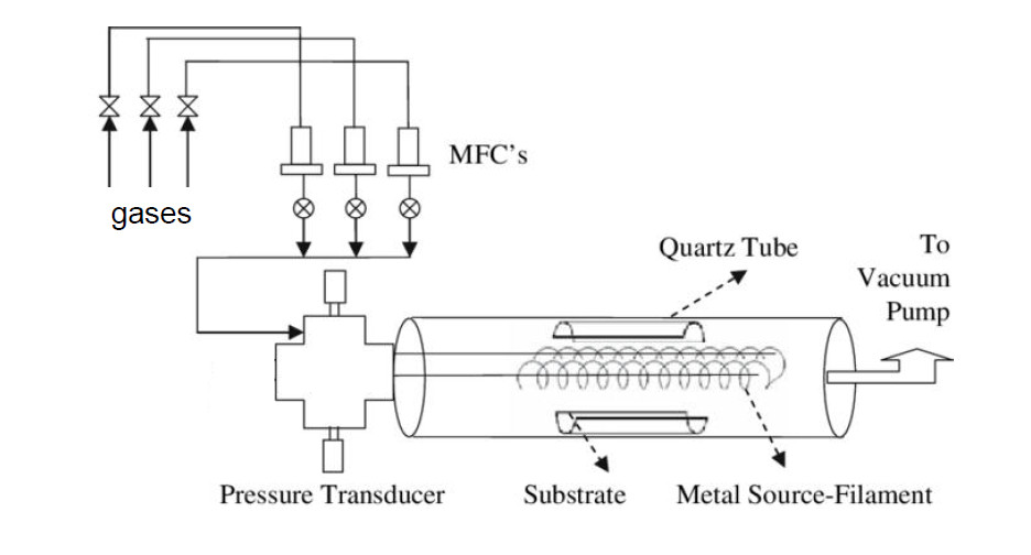
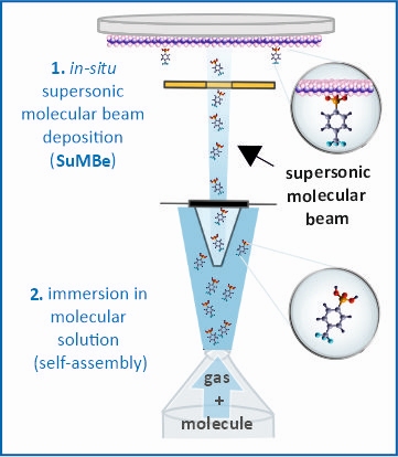
2D material growth technique |
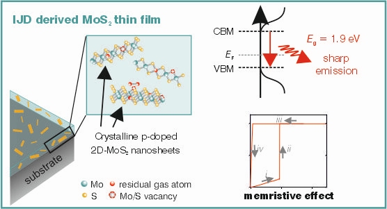
Highlight |
|
|
|
|
|
|