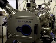


Thin films of wide bandgap semiconductors are deposited by vapor phase epitaxy:
|
|
|
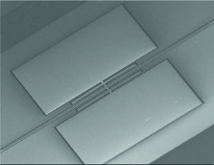
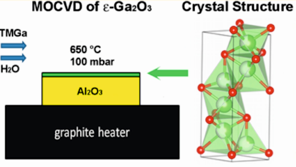
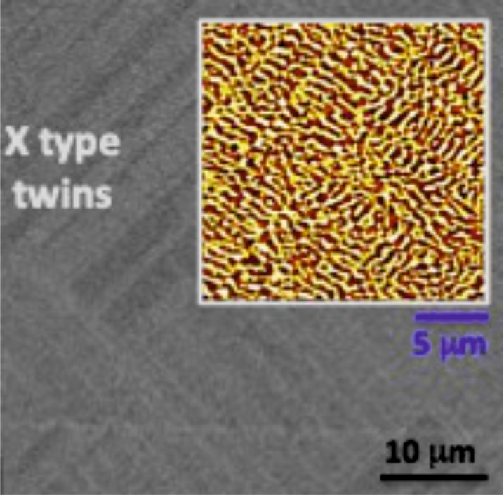
3C-SiC and Ga2O3 may be used in high power devices and in novel sensors.
|
|
We grow magnetic 3D metals and alloys as bulk materials or thin films, designing the single-phase or composite material to obtain the desired magnetic properties or study a specific physical problem. We have been able in several cases to achieve the control of the magnetic and functional properties by in-depth studying, and finally controlling, structure, microstructure and morphology. [...] |
|
|
Many materials can be successfully made with the PED pulsed electron technique; among these we point out:
|