


 CONTACT: Laura Lazzarini (laura.lazzarini@imem.cnr.it, tel 0521-269203)
Setup
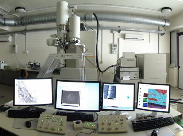
TEM JEOL JEM-2200FS with Schottky field emission gun. Performance:
- operating voltage: 80 kV, 200 kV
- point resolution: 0.183 nm (TEM), 0.132 nm (STEM)
- in column Omega filter
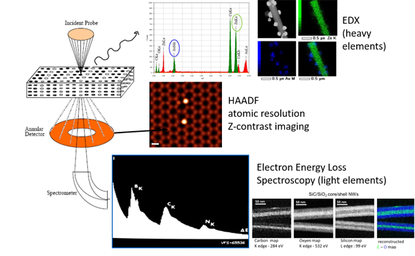
- two High Angle Annular Dark Field detectors (Z-contrast)
- Oxford detector (80 mm2) for EDX spectroscopy and imaging
For sample preparation:
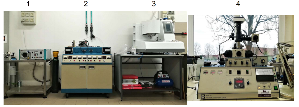
1. Plasma cleaner Femto (Diener Electronic) ; 2. Duo-Mill Ion Milling System (Gatan) ; 3. Advanced Grinding and Polishing System Accura 102 (Metkon) ; 4. Precision Ion Polishing System (PIPS), Mod 691 (Gatan). The equipment also includes a Buehler precision saw and a Gatan Dimple Grinder system.
Method
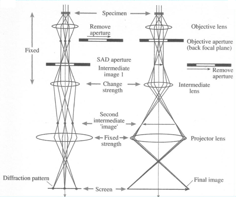
In both TEM and STEM mode, analytical techniques are also available:
- EDX spectroscopy and chemical mapping of elements. An X-ray detector placed above the sample allows the collection and the energy dispersion of the characteristic radiation emitted by the material, for spectroscopic investigations, compositional quantification and imaging of the spatial distribution of the elements.
- Electron Energy Loss Spectroscopy (EELS). By means of the in-column Omega filter, it is possible to analyze the electron dispersion in energy as a consequence of the interactions - elastic (zero-loss) and inelastic (e.g. ionization of the atomic shells, core-loss) - with the material passed through. The acquisition of EELS spectra and energy filtered images (EFTEM) is particularly interesting for the study of plasmonic modes, the valence state of some elements (e.g. Fe in oxides) and the presence and spatial distribution of light elements (e.g. C, N).
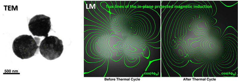
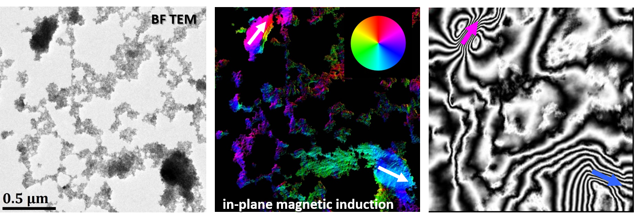
Lorentz microscopy (LM) is a method to map the in-plane magnetic induction in the thin foil. The technique is based on retrieving the phase distribution of the electron wave function by measuring the intensity distribution derivative along the beam propagation direction (through a series of images taken at different defocus values). To preserve the magnetic microstructure of the sample, the Lorentz microscopy is performed turning off the objective lens, thus limiting the spatial resolution to some nm.
Highlights
TEM techniques applied to magnetic materials
Advanced transmission electron microscopy techniques, including STEM-HAADF, HR-TEM and Lorentz microscopy, together with magnetic force microscopy (MFM-link), represent a powerful tool for the study of nanostructured magnetic materials. They can be employed to correlate the material properties at the macroscopic scale with the structural and magnetic properties at the micro- and nano-scale
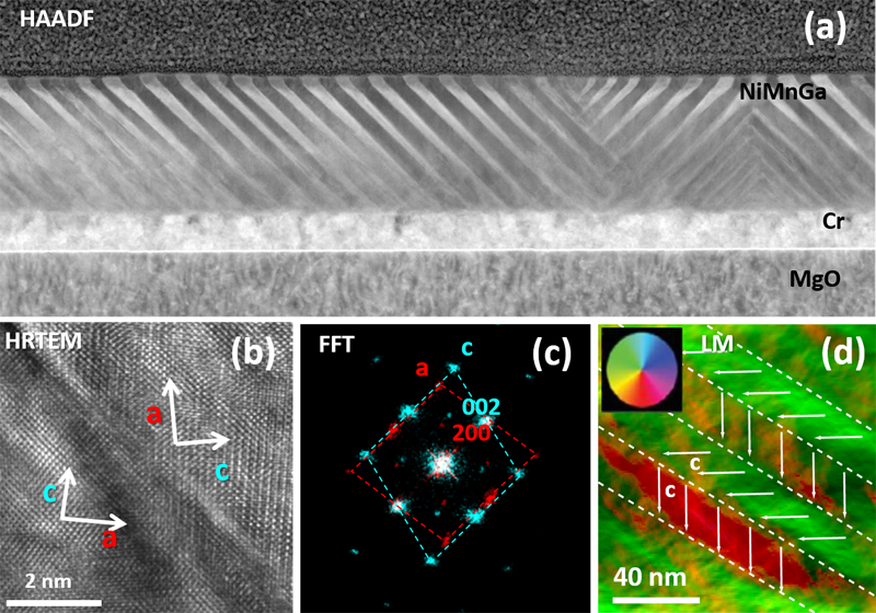
Refs: Acta materialia 2020, Advanced Materials 2015
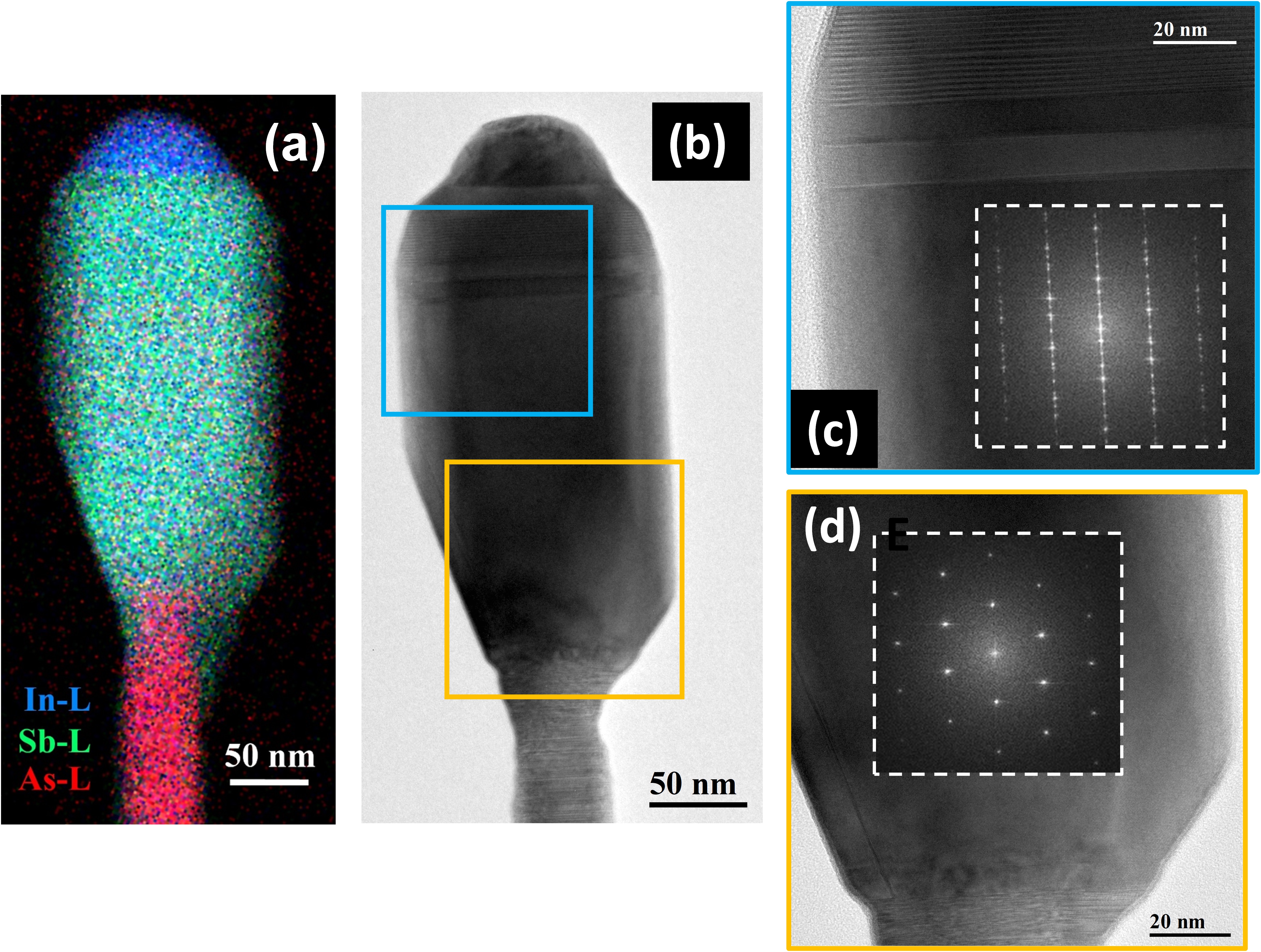
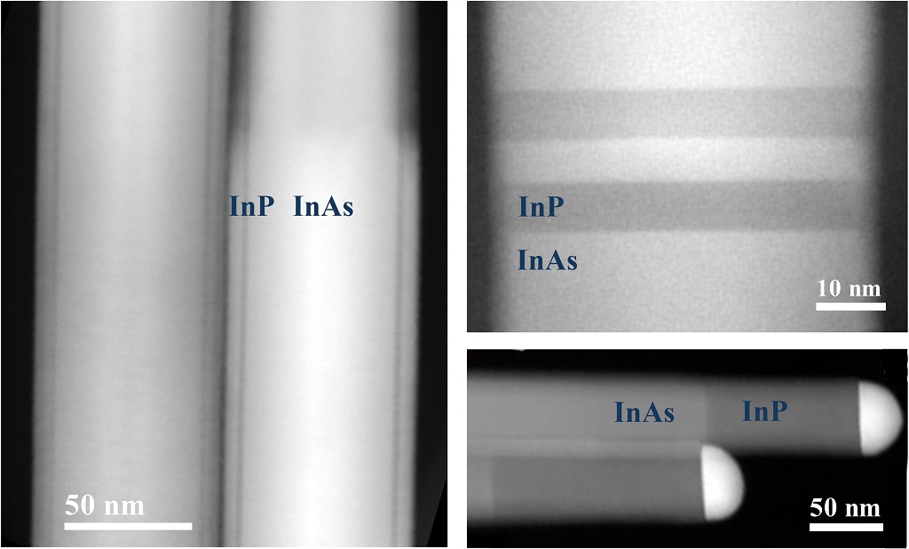
TEM techniques applied to nanowires
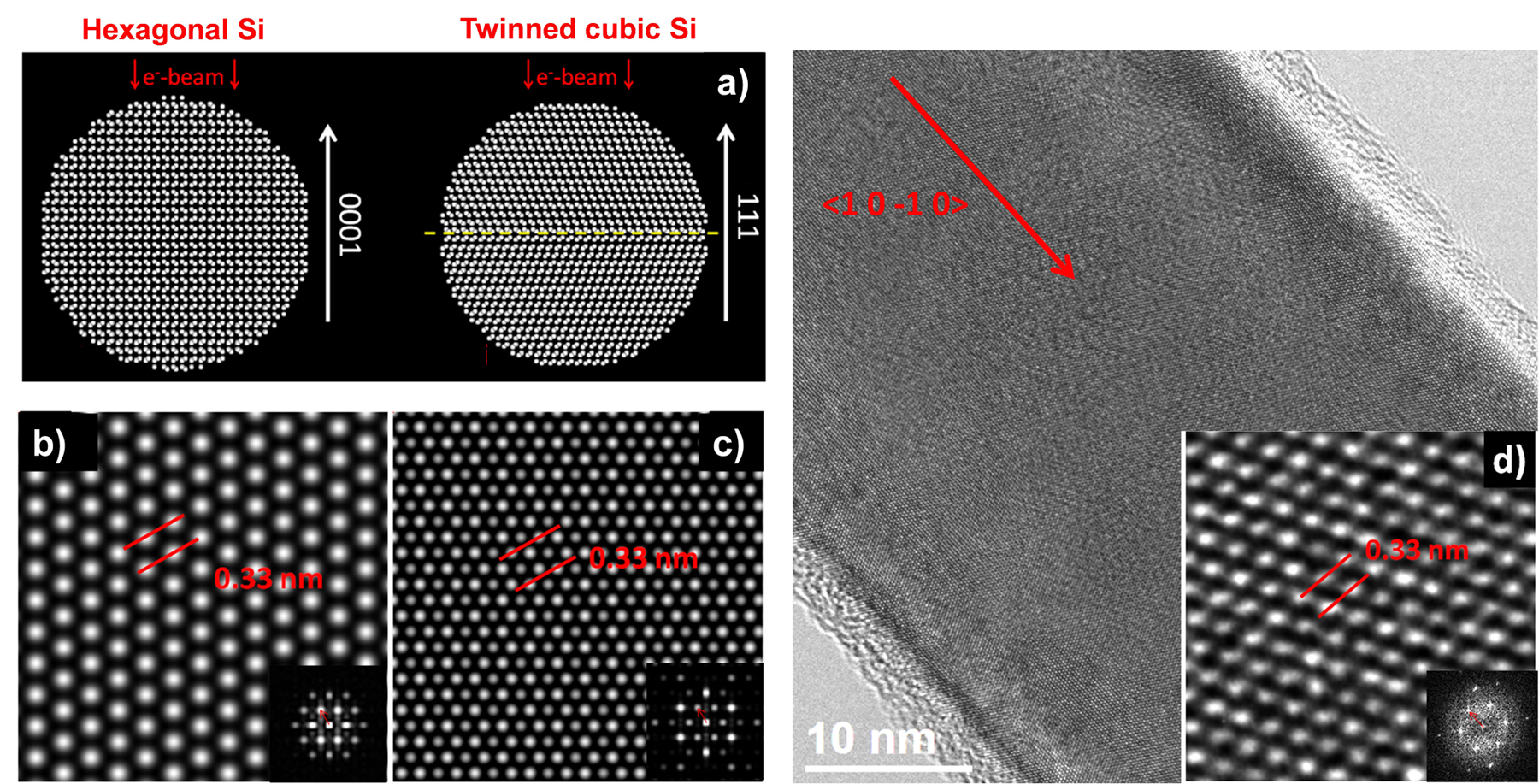
Hexagonal silicon has very promising optical properties, but it is difficult to prove the hexagonal phase by high resolution TEM techniques. In fact, defects in cubic silicon, for instance planar twins orthogonal to the 111 direction (upper left), viewed along particular directions, produce patterns that are similar to those of the hexagonal polytype. While the diffraction pattern is identical, the high resolution image is different, as clearly showed by simulations (bottom left). The experimental image on the right, compared to the simulations, allows to remove any ambiguity and to identify the hexagonal phase in Si NWs.
TEM-EELS spectroscopy of plasmon resonances in composite systems of nanostructured materials
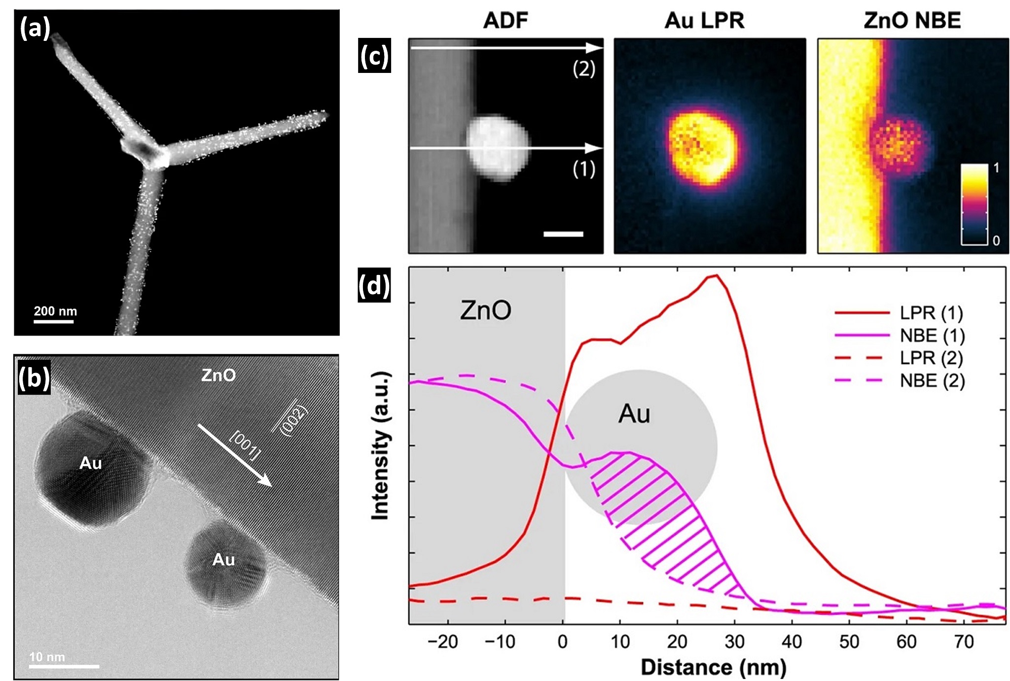
Experimental visualisation of the electromagnetic coupling between the plasmonic resonance (LPR) of a gold NP and the exciton (NBE) of its ZnO support by means of spatial mapping of the two emission distriìbutions. Ref: Sci. Rep. 2016
TEM techniques applied to multilayered solar cells
Analysis of photovoltaic cells
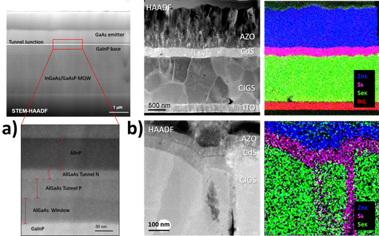
a) STEM-HAADF images of a III-V third generation MQW solar cell; b) Analysis of solar cells based on CIGS. The figure shows STEM-HAADF images of selected regions of the solar cell and the corresponding EDX elemental maps of Zn, S, Se and In.
TEM techniques applied to Carbon nanostructures
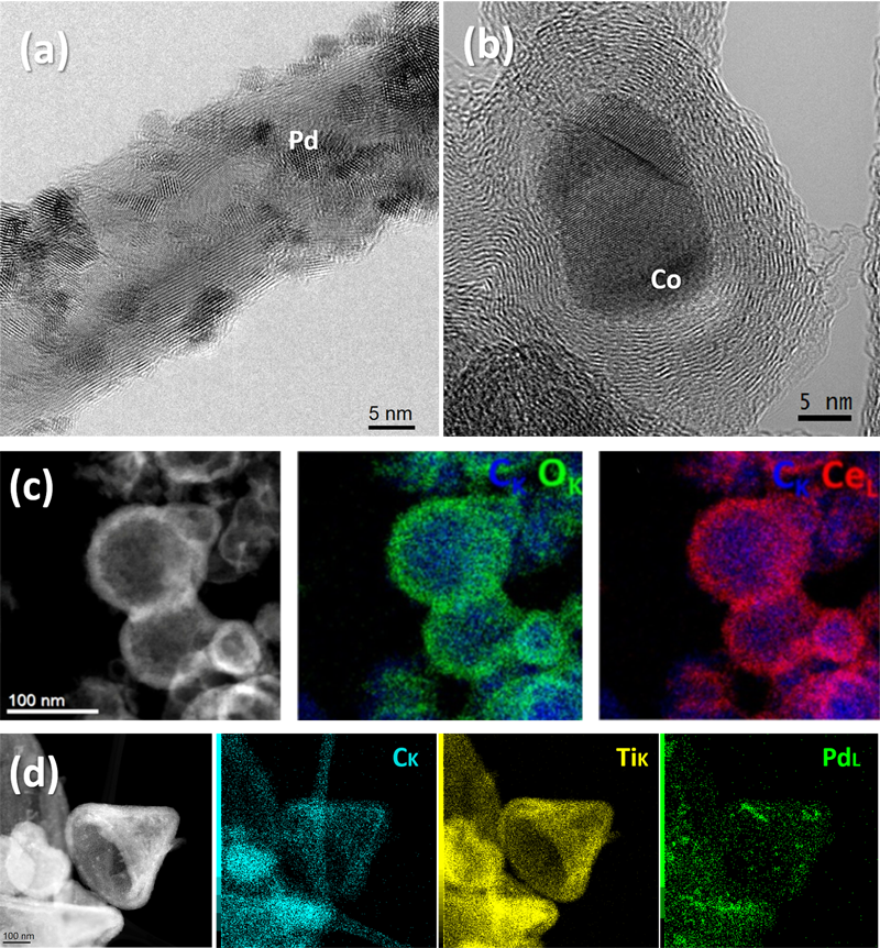
Analysis of hybrid systems based on carbon nanostructures, metal nanoparticles and metal oxides for electrocatalytic applications. a) HR-TEM image of a cobalt @ graphitic carbon core-shell nanostructure; b) HR-TEM image of a CNT/Pd@TiO2 nanostructure; c) STEM-HAAD image and corresponding EDX maps of carbon@CeO2 NanoHorns systems; d) STEM-HAAD iamge and corresponding EDX maps of carbon/Pd@TiO2 NanoCones. Refs: Sensors and Actuators B: Chemical 2017, CHEMSUSCHEM 2019, NATURE COMMUNICATIONS 2016, CHEMICAL COMMUNICATIONS 2016
project NANOREDOX- PRIN 2017
TEM imaging of organic materials
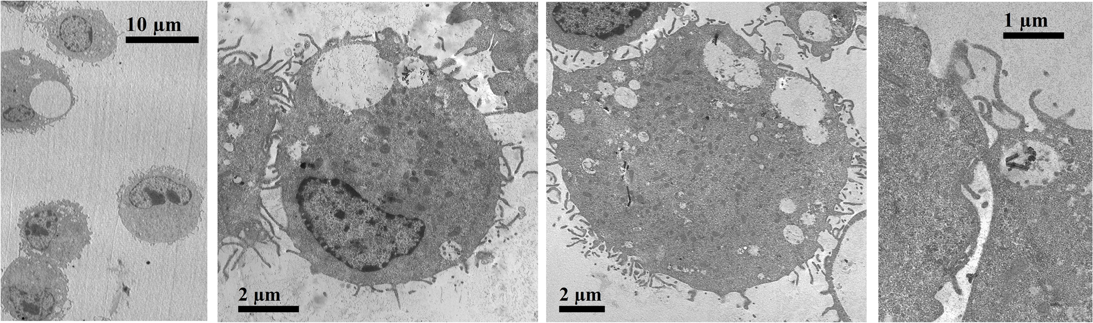
TEM imaging (working voltage 80 kV) of cells treated with nanowires for biomedical applications. Ref: Nano Letters 2014
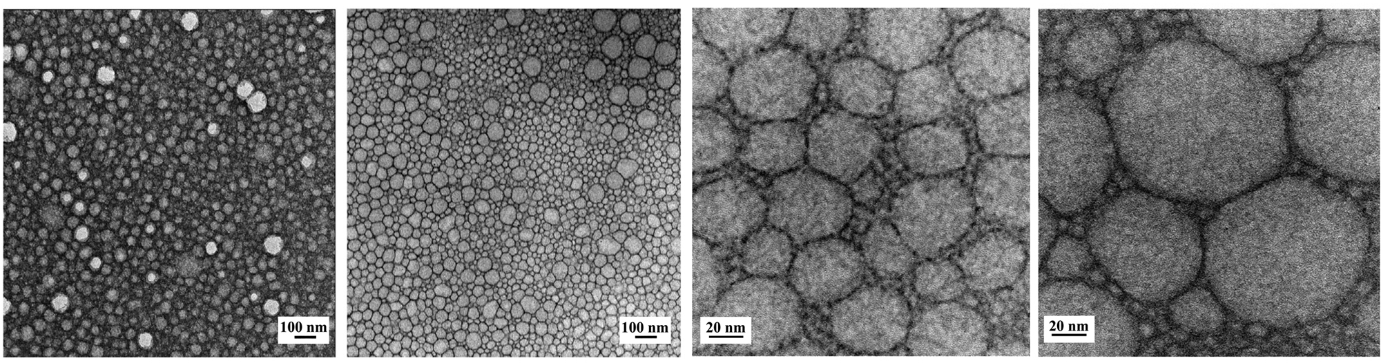
TEM imaging (working voltage 80 kV) of nanoformulations of farmaceutical interest. Refs: Eur. J. Pharmaceutical Sci. 2018, Pharmaceutics 2019