


 CONTACT: Lucia Nasi (lucia.nasi@imem.cnr.it, tel 0521-269285)
Setup
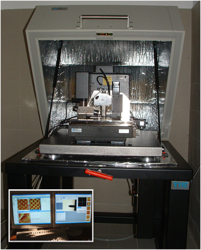
AFM Veeco Dimension 3100 Nanoman
Performance:
- AFM in contact mode
- AFM in tapping mode
- MFM Magnetic Force Microscopy
- SCM Scanning Capacitance Microscopy
- STM Scanning Tunneling Microscopy
- Nanolithography and Nanomanipulation (scanner closed loop)
Maximum scanning area: 100 µm x 100 µm
Sample size: up to 150 mm in diameter and 12 mm in thickness
Method
AFM in contact mode: a sharp tip at the end of a cantilever is brought in contact with a sample surface. The acttraction and repulsion forces between the tip and the surface produce a deflection of the cantilever which is detected by a laser-photodiode system. The distance between the tip and the sample is controlled by a feedback loop.The resulting map represents the topography of the sample surface. The lateral resolution depends on tip radius, typically a few nm, while the vertical resolution can be up to a few Å. The resulting map represents the topography of the sample surface. The lateral resolution only depends the tip radius, typically a few nanometers, while the vertical resolution can be up to a few Å.
AFM in tapping mode: the operating principle is similar to that in contact, with the difference that in this mode the cantilever vibrates at its resonance frequency so that the tip intermittently touches the surface of the sample. By detecting the amplitude or phase shift caused by the surface-tip interaction during the scan, the topography map of the sample is obtained. This mode of operation reduces the damage to the tip or sample and is particularly used to study soft material such as organic or biological ones.
MFM Magnetic Force Microscopy : in this mode the tip is coated with a thin layer of ferromagnetic material. By measuring the phase shift of the cantilever's oscillation induced by the magnetic tip-sample interactions, the map of the magnetic domains of the sample with magnetization perpendicular to the surface is obtained. To separate the magnetic contribution from the topographic one, a double scan technique is used (Interleave mode): during the first scan the topography is recorded, while in the second scan the tip is raised by a few tens of nm (Lift mode) and follows the morphology profile. During the second scan, the long-range magnetic interactions are detected.
SCM Scanning Capacitance Microscopy: with this technique, it is possible to measure, even quantitatively, local variations of the capacitance between a conducting tip and a conductive or semiconductor sample. It is particularly used to map semiconductor doping profiles with a lateral resolution of about ten nm.
STM Scanning Tunneling Microscopy: in this mode the sample topography is reconstructed by detecting the tunneling current that flows between the conducting probe and a conductive sample. The exponential dependence of the current on the tip-sample distance allows, in vacuum, vertical resolutions of a fractions of an Angstrom. To obtain such high resolution, the sample must be analyzed under vacuum to avoid the presence of contaminants on the tip and sample surface.
Nanolithography and Nanomanipulation: the precise control of the tip on the sample surface and the possibility of directly controlling the voltage between tip and sample, allow to manipulate the nanostructures by dragging the tip to the desired position and to oxidize the surface with nanometer precision.
Highlights
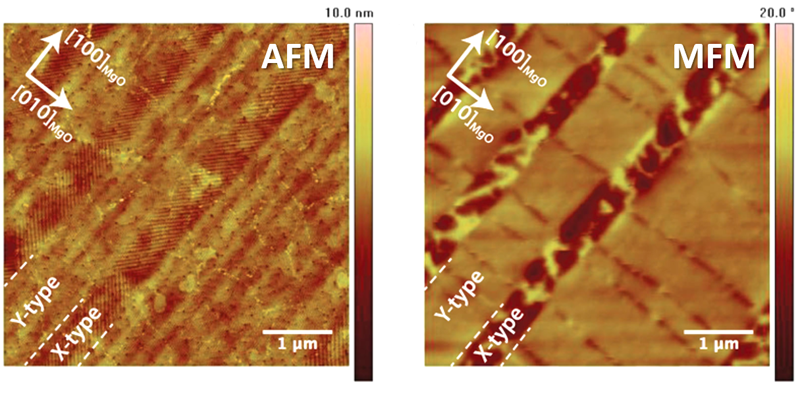
The AFM e MFM images show the presence of two regions with different morphology and magnetic configuration. The X and Y regions have magnetization perpendicular and parallel to the sample surface, respectively. Ref: Advanced Materials 2015
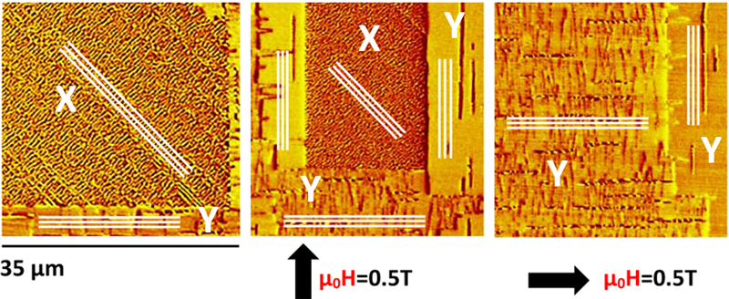
MFM analysis of a NiMnGa thin film carried out by applying a magnetic field along two perpendicular directions. Ref: Acta Materialia 2020