


 CONTACT: Lucrezia Aversa (lucrezia.aversa@cnr.it, tel +39 0461 314823)
Setup
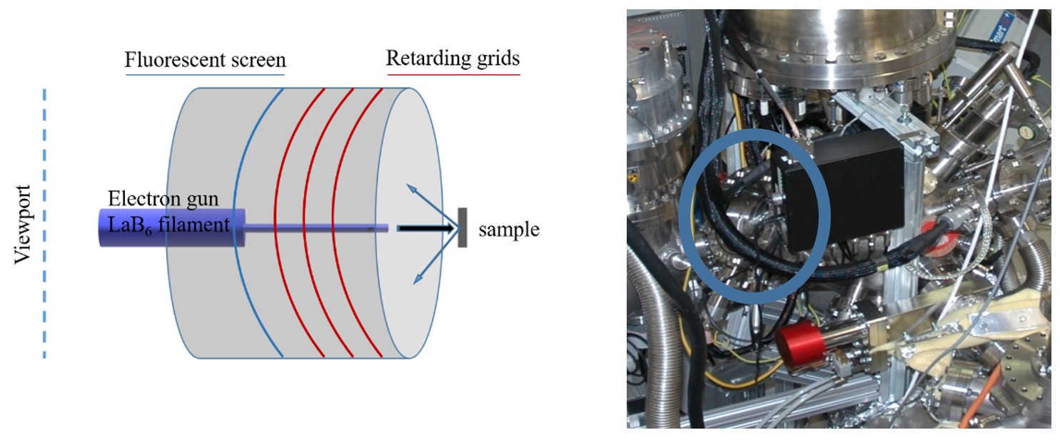
- Reverse view LEED with high brilliance LaB6 filament
- Retarding grids angular opening : 100° - 120°
- Electron beam energy : 10-1000eV (typically 20-200eV)
- Mounted on a UHV chamber equipped with XPS, AES and UPS techniques and connected to a supersonic molecular beam
Method
LEED (Low Energy Electron Diffraction) is a surface diffractometric technique based on the interaction between a low energy, collimated electron beam and a material, in order to assess its long range order and crystallinity.
Electrons with a kinetic energy of 10-1000 eV are characterized by a De Broglie lenght of few Angstrom, a lenghtscale comparable to crystalline parameters in solids ot thin films. Back-scattering of this electrons from the surface gives rise to diffraction of the first atomic layers, which pattern is detected through an hemispherical fluorescent screen.
Highlights
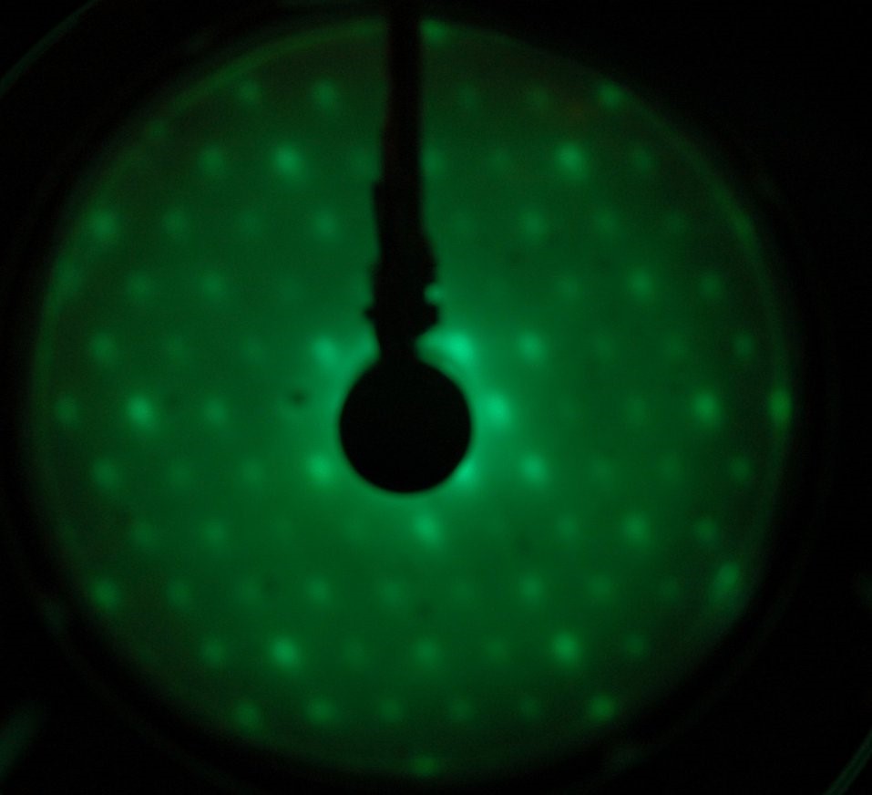
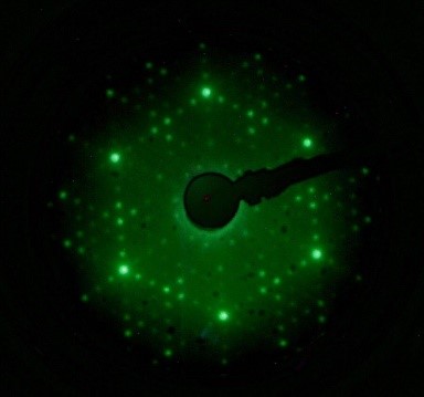
Identification of surface crystalline order and reconstruction after thermal treatments.
C60 (20nm) deposited on Cu and annealed at 425°C, E=80eV. The thermal treatment leads to desorption of fullerene, leaving a monolayer that reorganizes on the metal surface, assuming a long range order, deteactable by LEED. Ref: RCS Advances 2016
Oxydized Si(111) samples, annealed at high T and slowly cooled down, undergo oxyde desorption and surface reconstruction leaving a complex pattern characterized by a 7x7 periodicity; the high crystallinity is also revealed by the dark background and bright defined spots.
Identification of different crystalline patterns present on the surface (rotated domains, extrastructures)
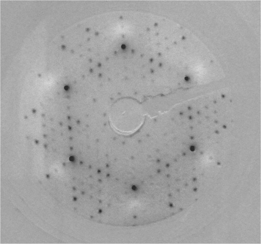
Epitaxial growth of submonolayer SiC on Si(111)-7x7 highlighted by the hexagonal pattern (brighter diffused extraspots) superimposed to the typical pattern of the reconstructed Si(111) surface. The low definition of SiC extraspots suggests the growth of nanocrystalline islands of some tens of nm. Ref: J. Am. Chem. Soc. 2012