


 CONTACT: Giovanna Trevisi (giovanna.trevisi@imem.cnr.it, tel 0521-269236)
Setup
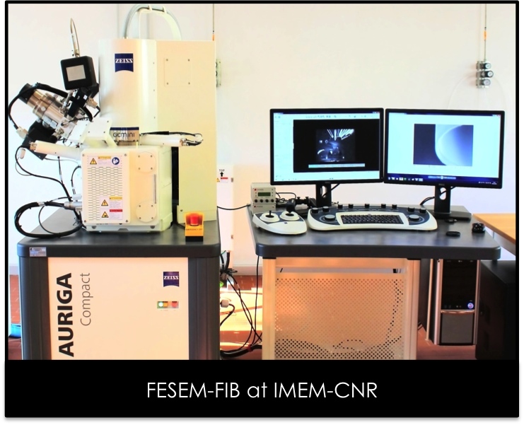
FESEM/FIB ZEISS Auriga Compact
- SEM: high resolution Gemini column with Schottky field-emission gun.
- FIB: high performance Canion column with Gallium liquid metal ion source.
- Detectors: InLens and Everhart-Thornley for secondary e-, BSD for backscattered e-, Oxford EDX (with 138 eV resolution) for compositional analysis.
- Single gas injection system and Pt precursor reservoir.
- Kleindiek micromanipulator.
Method
SEM operation: the generation of images in Scanning Electron Microscopy is based on the analysis of the interaction products generated by the primary electron beam impinging on the surface of the samples. By modulating currents and acceleration voltages of the electron beam and using the available detectors, it is possible to obtain different information: from morphology (SE and InLens detectors) to chemical composition (BSD and EDX detectors). The system allows to perform high resolution imaging for the study of nanostructured materials; it is also possible the use of low acceleration voltages (less than 1 kV) for the analysis of samples with low conductivity.
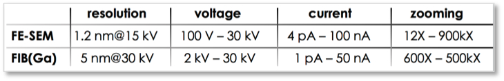
SEM-FIB operation: this working condition, also known as cross-beam operation, requires the sample to be placed at the coincidence point of the electron and ion beams. In this way, the area on which the ion beam impinges con be monitored in real-time by SEM imaging. This allows to accurately identify the position of the sample on which the FIB processing has to be performed and to control its evolution in real time. Some examples of FIB micro-processing are the following:
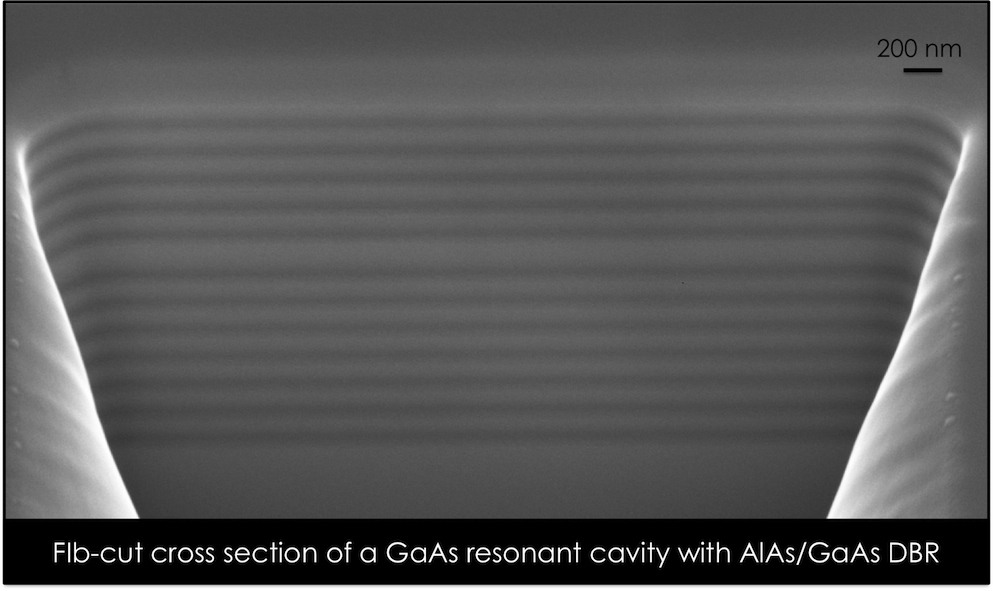
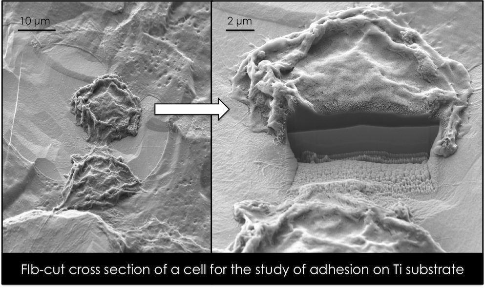
Cross-sectional analysis of materials. This procedure allows to evaluate the morphology and thickness of buried layers, to analyse the interfaces between different layers and to reveal the internal morphology of micro-structures. In this way, for example, it is possible to analyse not only the morphology but also the adhesion to the substrate of cells from in-vitro cultures, after an appropriate fixation, dehydration and metallization protocol.
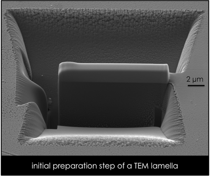
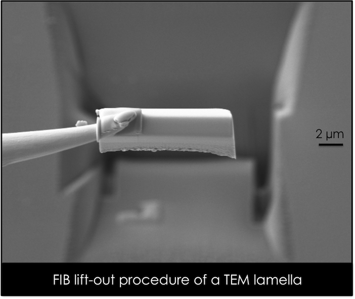
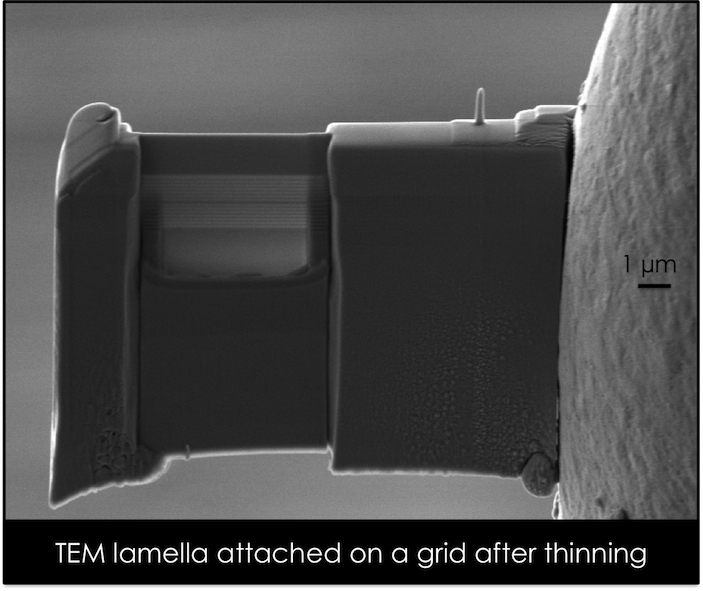
Preparation of TEM lamellae. This procedure allows to prepare high quality samples suitable for TEM analysis and consists of the following steps: extraction of a section of material, transfer to the TEM grid, thinning to electronic transparency and final cleaning of the interfaces. This complex procedure is necessary when the TEM analysis must be carried out on a specific area of the sample, but also when the samples cannot be treated using conventional preparation techniques.
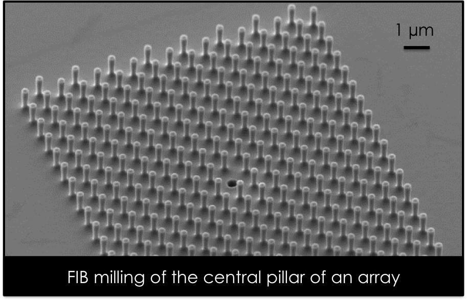
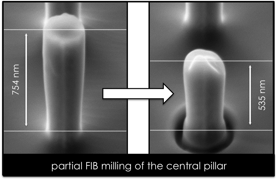
Milling of patterns on specific areas. This methodology is based on the high milling precision that can be obtained with the ion beam and can be assimilated to a micro-scale lithography without the need for resist and masks. It is therefore possible to transfer patterns of interest to the surface of the samples but also to modify pre-existing structures in a controlled manner, such as microelectronic circuits, lithography masks or arrays of microstructures.
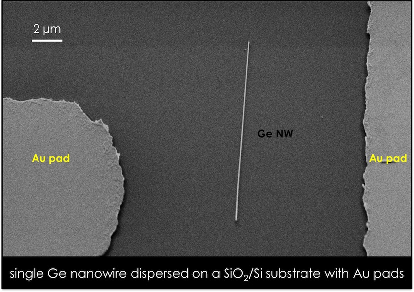
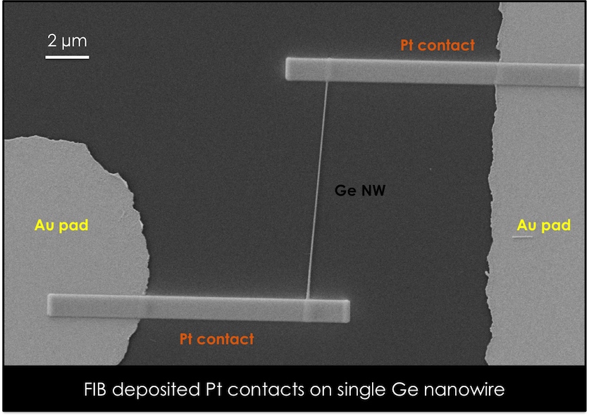
Metal deposition: through the single gas injection system it is possible to insert a gas containing a Pt precursor in close contact to the surface of the sample. Gas molecules are cracked as a consequence of the impact with the electron or ion beams giving rise to the deposition of Pt in the area where the interaction took place. Pt deposits obtained in this way have different uses. Usually they protect the sample surface before ion milling, a necessary procedure to prepare TEM lamellae, for example. Noteworthy, by choosing suitable ion beam parameters, Pt deposits can also be used as electrical contacts on a sub-micrometric scale.
Highlights
SEM/FIB techniques applied to cell cultures
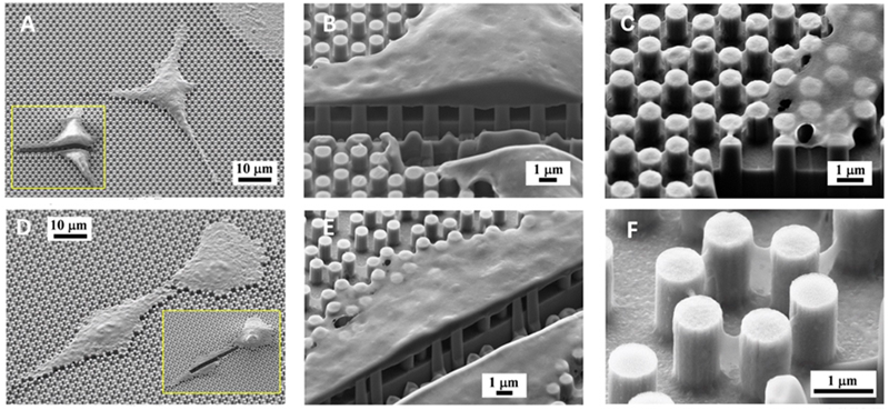
Analysis of morphology and adhesion mechanisms of MC3T3-E1 osteoblastic cells cultured on inorganic micro pillars. (A, D) SEM images of representative cells, before and after FIB cut. (B,C,E) Details of cell sections. (F) Typical morphology of the micro pillars after 48 h cell culture. Ref: Nanomaterials 2020