


 CONTACT: Letizia Savio (letizia.savio@imem.cnr.it, tel 010-3536292)
Setup
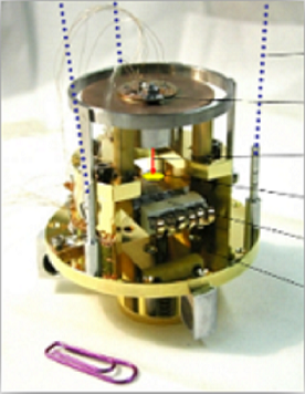 |
Scanning Tunneling Microscope (CreaTec). Low temperature operation: 77 K (LN2) or 6 K (LHe). |
|
|
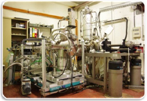
UHV setup equipped with the LT-STM. The microscope is coupled to a supersonic molecular beam. |
Method
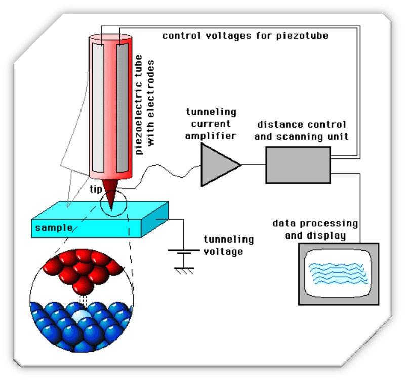
The STM technique is based on the quantum phenomenon of the tunnelling effect, whereby the current passing between a conductive or semiconductive sample and a metal tip placed at atomic distance from it is measured. By acquiring the reading of the «tunneling current» while the tip scans the surface, a map of the electronic density of the surface is obtained, which is correlated to its morphology. Depending on the operation conditions, the following information can be retrieved:
- Surface topography with atomic resolution
- Surface LDOS maps
- Spatially localized spectra of the LDOS around the Fermi level
- Manipulation of single atoms / molecules
Highlights
Determination of surface morphology
From the integrated LDOS map of the surface, the morphology of the surface is obtained, both in the case of metal / semiconductor surfaces and of supported ultra-thin layers (organic or inorganic). In the examples:
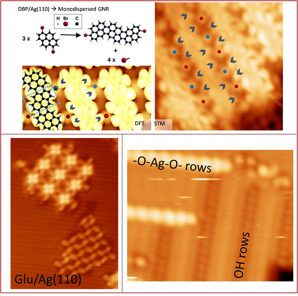
2) Self-assembly of glutamic acid on Ag(100). Refs: Langmuir 2010, Langmuir 2011, J. Phys. Chem C 2014.
3) OH/O/Ag(110), obtained by exposing O/Ag(110) to H2O. Ref: Phys. Rev. B 2006.
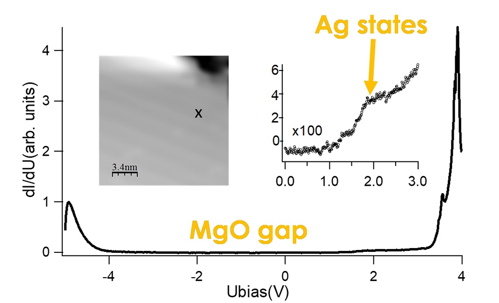
Scanning Tunneling Spectroscopy: LDOS measurement