


 CONTACT: Lucrezia Aversa (lucrezia.aversa@cnr.it, tel 0461-314823)
Setup
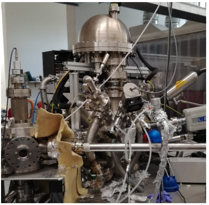
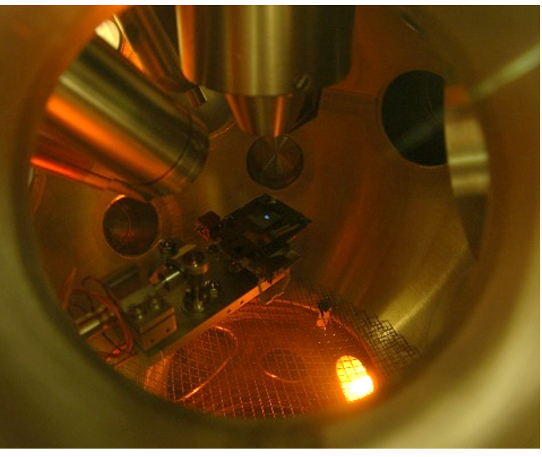
VSW HA100 analyser and PSP control unit @ IMEM-Trento
LEG62 ThermoVG electron gun
Maximum electron beam energy 5 keV
Maximum current 20 µA
Spot size up to 5 µm
Scanning Electron Microscopy (SEM) mode resolution ~3 µm
(detection of secondary photons emitted in the Auger process)
Method
This spectroscopy exploits the Auger effect in order to produce electrons from deep levels and it allows a surface chemical and compositional analysis. It is a three-particles process that brings to the emission of a secondary electron from valence levels after the excitation of a primary electron from a core level by means of an electron beam.
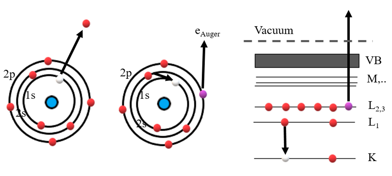
Complementary to XPS, this technique is able to probe shallow surface layers of conductors and semiconductors materials. It’s not applied to insulators or any material that easily decomposes under an electron flux.
Can be combined with sputtering techniques to obtain compositional depth profiles.
Highlights
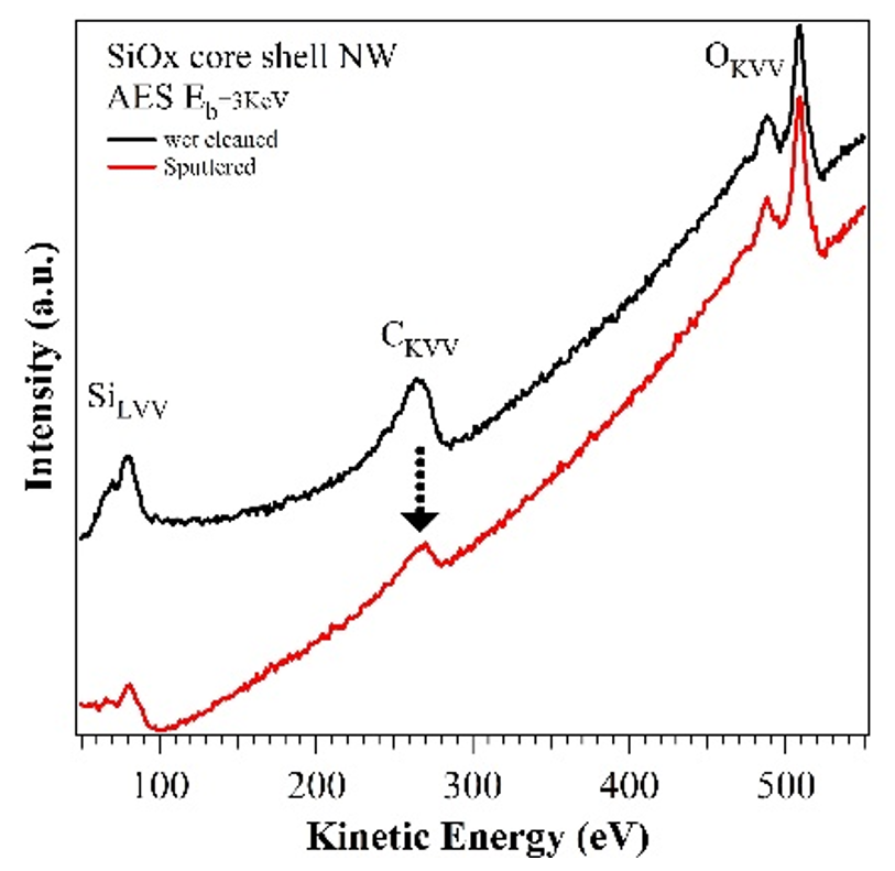
Silicon oxyde nanowires (SiOx) have been sputtered with an Ar ion beam to remove carbon contaminants. By means of AES it was possible to monitor the process and highlight some residual carbon due to cluster embedded into the nanowire.
This C induces luminescence processes when the nanowires are excited by the electron beam emitted by the “Auger source”. Ref:Nanotechnology 2014